Abstract: Introduces the basic characteristics of the high-performance audio digital-to-analog converter WM8741. An audio decoding circuit based on WM8741 and digital audio receiving device CS8416 is designed, and the interface design between CS8416 and WM8741 is given. The decoder consists of digital audio reception, digital-to-analog conversion, and analog signal conditioning. It supports up to 24-bit digital audio signal input with a frequency of 192 kHz. This article refers to the address: http:// 2 Introduction to WM8741 The WM8741 is a high-performance stereo digital-to-analog converter for high-end audio applications from Wolfson Microelectronics for professional audio systems, home theater, A/V receivers, CD/DVD players, and more. It has a dithered digital interpolation filter, fine resolution volume control and digital de-emphasis, a multi-bit sigma-delta modulator and a switched-capacitor multi-bit circuit stage with differential voltage output. The unique programmable digital high-level digital filter allows the user to flexibly select group delay, phase delay, impulse response, and more. The audio input interface supports I2S, Left-justifted, Right-justified and DSD formats. When inputting as a PCM signal, the device can receive a word length of 16 to 32 bits and a sampling conversion rate of 32 to 192 kHz. The device has both hardware and software control and is switched by an external pin. In software control mode, the external CPU accesses all its internal registers and sets parameters through 2-wire or 3-wire mode. With a signal-to-noise ratio of 128 dB (mono), the WM8741 has a dynamic range of 125 dB, a channel separation of 130 dB, and a power supply rejection ratio of -80 dB (100 mVpp, l kHz). The converted analog voltage is output in differential mode. The digital part of the WM8741 has a supply voltage of 3.0 to 3.6 V and a rated operating voltage of 3.3 V. The analog part has an operating voltage of 4.5 to 5.5 V. The rated operating voltage is 5.0 V. The device is available in a 28-pin SSOP package. 3 decoder hardware design The CS8416 has multiple optional audio input connectors. The system design is to connect the pin RXSEL1 of the CS8416 to the high level, the pin RXSEL0 to the ground, and the pin RXP3 as the audio data input interface. Audio clock reconstruction is achieved by an on-chip phase-locked loop (PLL) that locks the sampling frequency Fs in the input audio data over a wide range without excessively changing external components. However, the filter circuit composed of external resistors and capacitors also affects the frequency variation range. In order to obtain a low jitter reconstruction clock, the external capacitor's resistance and capacitance values ​​are shown in Figure 2. 4 Conclusion Designed to implement a digital audio decoder with a 24-bit, 192 kHz sampling rate. The decoder does not require MCU control, and the circuit is simple and stable. However, due to the hardware control mode, the circuit configuration has certain limitations. If you want to further increase its function, you can add a MCU and adopt software control mode to realize human-computer interaction. The WM8741's superior performance allows the decoder output to have a high dynamic range with very low noise for different audio products.
Description of Stacked D-Sub I/O Connectors
Range of of Stacked D-Sub I/O Connectors
Male Stacked D sub Connector
Dual Port (Stacked) D Sub,,Stacked D Sub I/O Connectors,Dual-Port Stacked D-Sub Connectors,Male Stacked D sub Connector, Female Stacked D sub Connector, Standard Stacked D sub Connector, High Density Stacked D sub Connector ShenZhen Antenk Electronics Co,Ltd , https://www.antenkwire.com
Keywords: audio decoding; digital-to-analog conversion; WM8741; CS8416; I2S
1 Introduction Audio decoders are widely used in everyday life. The requirements for audio decoder performance vary widely from application to application. There are many factors that affect sound quality, such as audio encoding format, transmission mode, and performance of codec devices. Digital-to-analog conversion is a key part of the decoding circuit, and its performance directly affects the quality of sound playback. In order to obtain high-quality analog sound signals, an audio decoder design based on the high-performance stereo digital-to-analog converter WM8741 is designed. The system supports digital audio signal decoding up to 24-bit and 192 kHz, and supports various other speeds. The input of a standard digital audio signal.
3.1 Hardware Composition Figure 1 is a block diagram of the decoder hardware structure. The digital audio receiver uses Cirrus Logic's high-speed digital audio receiver CS8416, which supports multiple audio inputs including S/PDIF, sampling frequency range. It is 32 to 192 kHz. The CS8416 is connected to the WM8741 via an I2S interface. The I2S bus only processes audio data, and other control signals must be transmitted separately. The working principle of the CS8416: The receiver decodes and converts the received digital audio data in S/PDIF format, and reconstructs the clock in the audio data and provides it to the subsequent WM8741. The audio data is sent to the WM8741 through the I2S bus interface. After the WM8741 completes the digital-to-analog conversion according to the set parameters, the analog audio signals of the left and right channels are output in differential form, and the high-frequency harmonic noise is filtered out by the low-pass filter, and finally a high-quality analog voltage signal is obtained. If the output interface is RCA, you also need to convert the differential signal to a single-ended signal. 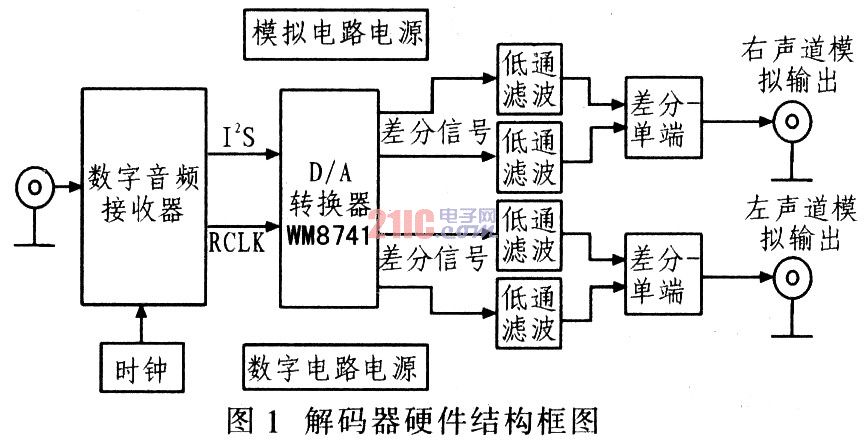
3.2 Digital Audio Signal Receiving Module The CS8416 is the core of the digital audio signal receiving circuit. In software control mode, the MCU has no parameters through the SPI or I2C interface. This mode also gives you the flexibility to change the internal configuration. In the absence of an MCU, control is achieved by changing its specific pin level by hardware control. Since there is no MCU in this system, hardware control is adopted. Use a 47 kΩ resistor on the SDOUT pin to pull it to ground, and the pins AUDIO, RCBL, U, C, etc. cannot be left floating, and must be pulled high or pulled low through a 47 kΩ resistor. For system reset, the CS8416 determines its operating state by detecting these pin levels. Table 1 shows the configuration of the control pins for this system design. 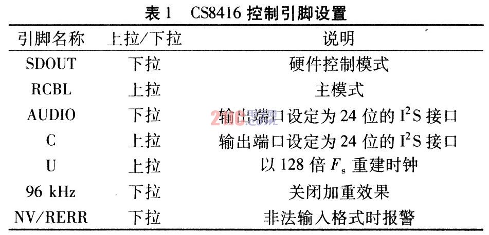
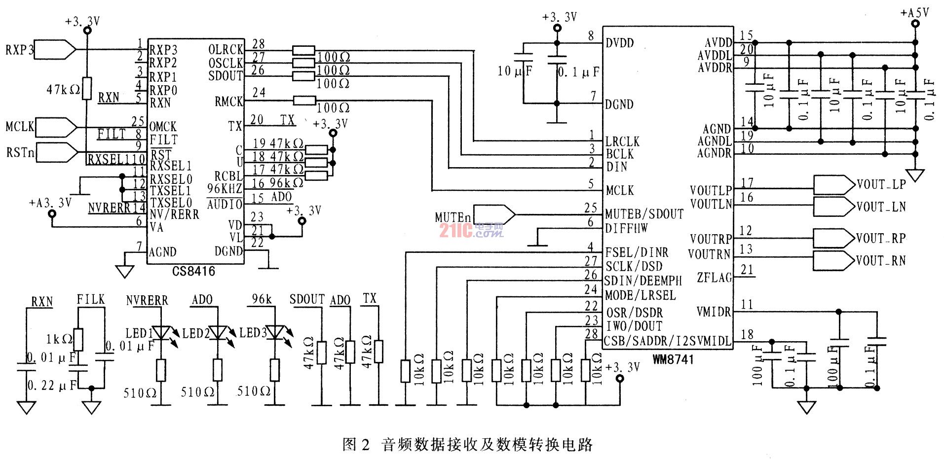
3.3 Digital-to-analog conversion module The I2S input interface of the WM8741 is connected to the output of the CS8416 with a 100 Ω resistor for buffering, as shown in Figure 2. The WM8741 sets the hardware control mode, which determines its operating state by the pull-up or pull-down status of a specific pin, and all pull-up or pull-down resistors are 10 kΩ. The WM8741 control pin settings for this system design are shown in Table 2. 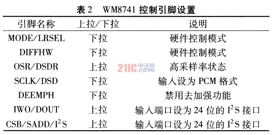
The main clock detection circuit inside the WM874l automatically determines the relationship between the main clock MCLK and the sampling clock LRCLK, and determines the final sampling rate. Although the WM8741 allows MCLK to have some phase delay and jitter, it should be designed to synchronize MCLK with LRCLK. After the digital-to-analog conversion is completed, the pins VOULP and VOULN output the differential analog voltage signals of the left channel, and the pins VOURP and VOURN output the differential analog voltage signals of the right channel. The WM8741 digital circuit operates at 3.3 V and the analog supply voltage is 5 V. All power supply pins are connected to a 10μF tantalum capacitor and a 0.1μF ceramic capacitor for decoupling filtering. A magnetic bead is connected between the digital ground and the analog ground to reduce interference.
3.4 Analog Signal Conditioning Module The analog signal outputted by the WM8741 is mixed with higher harmonic components. Therefore, low-pass filtering is required to filter out high-frequency noise, resulting in a purer analog signal. The filter circuit uses an LM4562 operational amplifier. For digital-to-analog conversion circuits, a 3rd-order filter is required behind the D/A converter to achieve anti-aliasing requirements. A third-order Butterworth low-pass filter consisting of an LM4562 external resistor and capacitor is shown in Figure 3. The filter is unity gain and has good flatness in the passband. The filtered signal can be directly output as a balanced signal of the decoder. When outputting with the RCA interface, the differential signal needs to be converted into a single-ended signal. The conversion circuit is a differential amplifying circuit composed of a piece of LM4562. The single-ended signal is output to the RCA interface via a 10μF DC blocking capacitor. The LM4562 operates from a separate ±12 V supply. 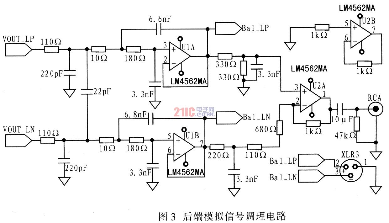
3.5 Problems to be Noticed in Design When drawing PCBs, pay attention to proper layout. Digital components and analog components should be placed separately. The layout of the external filter resistors of the CS8416's phase-locked loop affects the quality of the audio clock reconstruction. The capacitors should be placed as close as possible to the FILT pins, and preferably on the same plane. It is best not to have vias nearby.
Antenk's connectors are designed for applications requiring multiple connector ports with limited PCB space
The condensed footprint of Antenk's dual port D-sub solution is available in four industry sizes, three connector spacing options, and six hardware configurations for one of the broadest stacked D-sub offerings on the market in standard and high-density variations.
Stacked D-sub I/O connectors are designed for applications requiring multiple connector ports with limited PCB space. Two right angle D-sub connectors are stacked one on top of another, creating a single dual-port connector with a very condensed footprint.
Features of Stacked D-Sub I/O Connectors
Available in four industry standard sizes:
Standard density: 9, 15, 25, 37
Available in three connector spacing options: 0.625", 0.750", 0.900"
Available in six hardware configurations
High-temperature UL94 V-0 thermoplastic (260°C process temp)
High performance stamped contacts
Applications of Stacked D-Sub I/O Connectors
Communications
Instrumentation
Medical
Computers/peripherals
Commercial industry
Test labs
Gaming industry
Standard Density Stacked D sub Connector
High Density Stacked D sub Connector
Dual-Port Stacked D-Sub Connectors
December 20, 2023