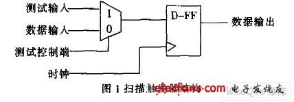
In order to ensure the correctness of the chip after the completion of the production, this problem related to circuit testing is getting more and more attention. Moreover, the difficulty and cost of the test are getting higher and higher, so how to effectively verify the correctness of the circuit and greatly reduce the test cost has become a hot topic of our research. Usually, we design the chip at the same time, according to the characteristics of the chip itself, additionally designability test design (Design For Testability) in the chip. Circuit design that talks about testability, built-in self-test (BIST) and scan-based Scan-Based circuit design is often mentioned. Scan-based circuit design is one of the most commonly used methods in testability design. It is a circuit belonging to the Test-Per-Scan test method. There are two current test methods, one is Test-Per-Scan and the other is Test-Per-Clock. Both test methods have their own advantages and disadvantages. The so-called Test-Per-Scan works by connecting all or part of the registers in a circuit to form a scan chain, and then shifting the test sequence into a value every cycle until the test vector fills the entire scan path. After another cycle, we pass the test results of the circuit under test to the scan chain. Finally, remove and do the compression analysis. The advantage of this method is that it can be easily applied in any commercial design process, and its hardware architecture has less impact on system functions. The control hardware design is also simpler: the disadvantage is that * more time is needed to generate test vectors. The test is slow. The so-called Test-Per-Clock, when we are testing the circuit, each cycle sends a new test vector into the circuit, and at the same time the output of the circuit is tested, so the circuit test time is shorter in this way. , faster. Scan-based circuit design, mainly to replace all or part of the registers in the circuit under test with scan registers, so that we can easily control the input and output when testing the circuit. The most common structure of the scan register is Multiple scan registers, which are added to a multiplexer on the input port of a normal register, as shown in Figure 1. The test control end is the selection end of the multiplexer, and the data input end is a normal function input end. There are also test inputs, clock inputs and data outputs. When the test input is "0", the register is the normal function input, the circuit is in the normal mode; when the test input is "1", the register is the scan input. The circuit is converted to scan mode. It is clear. Scan-based circuit design can increase the controllability and observability of the circuit under test. This design approach. The advantage is that it requires less extra hardware space, and the test results are better. The disadvantage is that the test time is too long. There are several reasons for the long test time, which we can obtain by analyzing the scan-based circuit design. This shortcoming is exactly what we want to improve. 2 basic unit of scanning based circuit 2.1 Linear Feedback Shift Register (LFSR) The simplest test vector generator is composed of Linear Feedback Shift Registers (LFSR). Because the value of the D flip-flop in the linear feedback shift register changes when the clock signal changes, we can use these values ​​that will change all the time as test vectors and send them to the circuit for testing. The general linear feedback shift registers can be divided into two categories, the Extemal XOR linear feedback shift register and the Internal XOR linear feedback shift register, as shown in Figure 2. The main difference between the two linear feedback shift registers is that the modulo-2 adder of the External XOR linear feedback shift register is placed on the feedback path of the circuit. The adder of the Internal XOR linear feedback shift register is placed in two registers. The test vectors generated by these two different linear feedback shift registers are also different. The test vector generated by the ExternalXOR linear feedback shift register has the following characteristics: the relationship between each vector and the next vector is a vector. The bits in the middle are shifted to the right by one. The linear feedback shift register of Internal XOR is because the modulo-2 adder is in the register, so the generated test vector looks more random than the External XOR linear feedback shift register, so we must select InternalXOR LFSR as the test. Vector generator.
Draw-wire sensors of the wire sensor series measure with high linearity across the entire measuring range and are used for distance and position measurements of 100mm up to 20,000mm. Draw-wire sensors from LANDER are ideal for integration and subsequent assembly in serial OEM applications, e.g., in medical devices, lifts, conveyors and automotive engineering.
Linear Encoder,Digital Linear Encoder,Draw Wire Sensor,1500Mm Linear Encoder Jilin Lander Intelligent Technology Co., Ltd , https://www.jllandertech.com

June 10, 2024