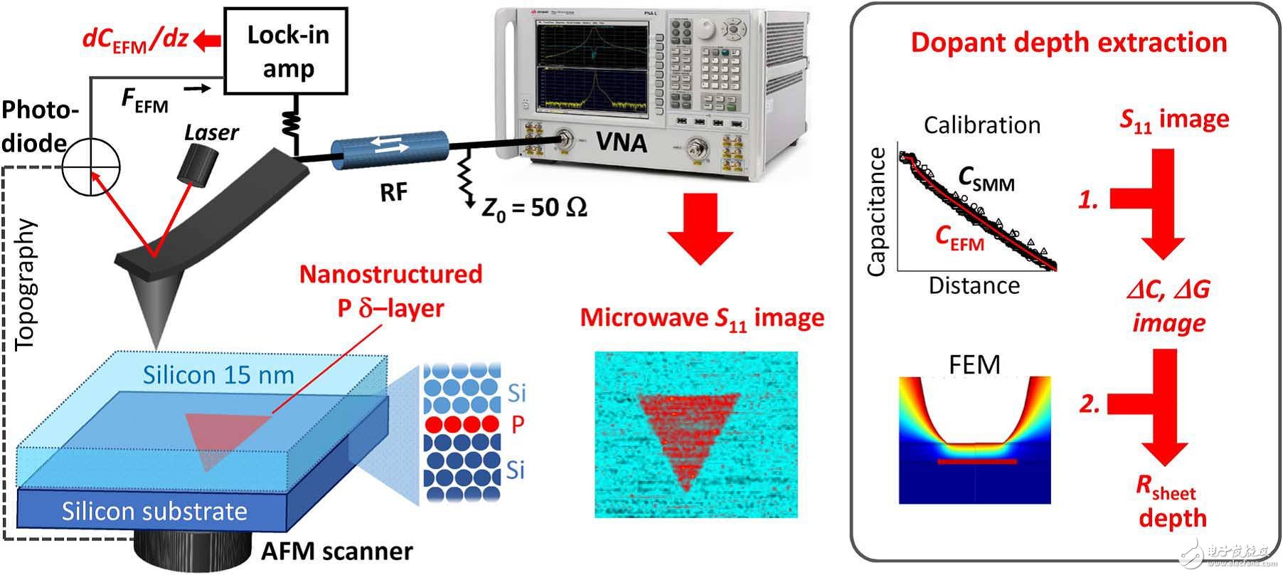
The international team from the University of Linz in Austria, University College London, the Federal Institute of Technology in Zurich and the Federal Institute of Technology in Lausanne, Switzerland, applied the existing microscopy technology, Scanning Microwave Microscopy (SMM), to silicon chips. In the detection of artificially incorporated impurities, the entire imaging process does not cause any damage to the chip (the semiconductor will be doped with impurities to enhance its conductive and optical properties).
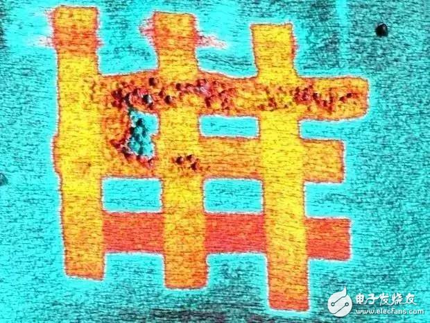
Phosphorus-silicon material imaging
The researchers used a scanning microwave microscope to scan the samples and specifically examined the electrical properties of the phosphorus atoms arranged in a regular pattern under the surface of the silicon crystal. Under this method, the researchers successfully detected 1900-4200 closely packed atoms below the surface of 4-15 nm.
Of course, techniques such as Secondary Ion Mass Spectrometry (SIMS) can also be used to detect artificially incorporated impurities in semiconductors, but the main advantage of scanning microwave microscopy is that it does not cause any damage to the sample. .
In an email interview with IEEE Spectrum, Georg Gramse, the leader of the lab and the University of Linz, Austria, said:
"From the new technology for scanning silicon chips, we can anticipate potential impacts on the global industry. Because in the case where the chip integrated circuit is getting smaller, the measurement process has become extremely difficult and time consuming, and may damage the chip itself.
â€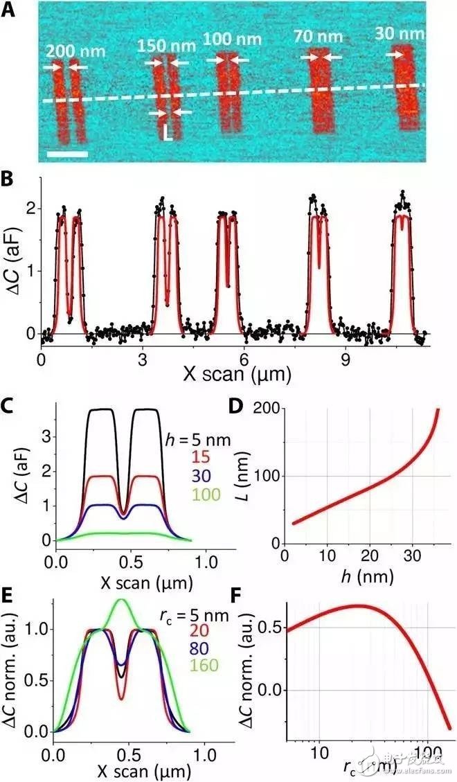
SMM and VNA measurement results for materials

New imaging technologies have laid the foundation for the implementation of phosphor-silicon quantum computers because of the ability to integrate scanning microwave microscopes into existing detection instruments. This will greatly speed up the fabrication of three-dimensional structures because the technique can also be applied to iterative control of atomic doping in lithography processes.
Gramse finally said:
" At the moment, we are studying the physical properties of the phosphorus atomic layer, which will be the next step to the phosphorus-silicon quantum computer. "DC Motor,Quiet And Strong Wind,Turbo Air Circulator Fan
Foshan Shunde Josintech Electrical Appliance Technology Co.,Ltd , https://www.josintech.com