Design of MT-ZigBee hardware platform 0 Introduction ZigBee technology is a short-distance, low-rate wireless communication technology with a unified technical standard. Its physical layer and media access control layer protocols are IEEE 802.15.4 protocol standards. The network layer is formulated and applied by the ZigBee technology alliance. The development of the layer is designed according to the actual application needs of the user. 1 ZigBee hardware solution In the ZigBee technology alliance, Freescale, TI, Chipeon, Philips and other companies are the pioneers of ZigBee standard formulation. In terms of RF transceiver chips, there are mainly two solutions provided by Freeseale's MC13192 and MC13193 and Chipeon's CC2420 and CC2430. The following is a simple comparison of these two optional hardware development solutions. 2 MT-ZigBee hardware platform design The MT-ZigBee hardware platform design mainly includes hardware platform selection, ZigBee control circuit hardware design and ZigBee RF circuit part hardware design. 2.2.1 Power input module The wireless sensor network is mainly used to collect field data and then perform corresponding control. The equipment is placed on the collection site. Considering that it is easy to carry and install, the power supply uses 1 9 V dry battery. On the hardware circuit, the power supply is divided into two ways: one way is the power supply for the main control chip GB60; the other way is the power supply for all peripheral modules such as LCD, MC13192, SCI, buttons and test lights. The specific power supply circuit is shown in Figure 2. In the power supply circuit, the power supply of the main control chip exists under any circumstances. This ensures that the GB60 is working in any case; the peripheral module power is controlled by the main control chip, and the GB60 controls the peripheral module power through the MOS tube: when the system is working normally, the GB60 allows the peripheral module power to be powered on; when the system enters low power consumption In the state, GB60 cuts off the power supply of peripheral modules. In this way, only the main control chip of the entire system is powered, and then the main control chip enters the low power consumption mode (Stop Mode), so that the low power consumption of the entire system is better achieved. Note that when the power supply of the peripheral module is cut off, the general transistor cannot be used directly, so that the peripheral module still has a large current consumption after entering the low power consumption state, and it should be realized by using a MOS tube (such as SI2301) with good current cut-off performance. The G1360 reads and writes the registers on the MC13192 and the on-chip RAM through the standard 4-wire SPI interface. During communication, MC13192 can only be used as a slave. Therefore, for MCU, the MOSI line is the transmit data line, and the MISO line is the receive data line. The SPI synchronization clock is given by GB60 on the SPSCK pin, and is connected to the SPICLK of MC13192 on. (2) The design of the antenna circuit. There are three types of antennas for 2.4 GHz RF circuits: external upright antennas, PCB antennas and chip antennas. The performance of the external upright antenna is the best, but the volume is too large, and it can only be used in occasions where there is no requirement for the volume; the chip antenna is implemented with integrated circuits, the performance is general, and it is difficult to adjust the performance according to the actual situation; However, it has high requirements on design and PCB wiring, and is most used on the hardware platform of wireless sensor networks. 3 MIT-ZigBee hardware platform module test After completing the hardware circuit design, the hardware circuit of each module must be tested to ensure the reliability of the hardware circuit. For the entire hardware circuit, it should be soldered and debugged separately according to the module, and debugged by module and then combined together for debugging. It is necessary to reserve a certain test node when designing the hardware PCB for later measurement and use. 4 conclusions Here mainly provides the corresponding hardware platform design for the realization of ZigBee protocol stack. Based on the hardware chip selection of the MT-ZigBee platform, the overall framework of the hardware platform is given, and the detailed design of the hardware platform power circuit, GB60 and MC13192 interface circuit, and MC13192 RF module are described. Finally, the modules of the MT-ZigBee hardware platform were tested. Due to the limited space, the application examples of implementing the underlying protocol stack design related to ZigBee technology and specifically verifying the availability of the protocol stack are not introduced here. Cylindrical Battery,Cylindrical Shell Method,Cylindrical Batteries,Cylindrical Battery Cells Langrui Energy (Shenzhen) Co.,Ltd , https://www.langruienergy.com
Before designing and developing the ZigBee protocol, there must be the support of the corresponding hardware platform. Here, the corresponding hardware platform design is provided for the realization of the ZigBee protocol stack. This article mainly introduces the design of MT-ZigBee hardware platform and the test of each hardware module. The design of the hardware platform mainly includes the selection of the hardware platform, the hardware design of the ZigBee control circuit and the hardware design of the ZigBee RF circuit part; the testing of the hardware platform mainly includes the testing of each hardware module.
Freescale has launched a complete hardware solution for ZigBee technology, which mainly includes MC13192, MC13193 radio frequency (Radio Frequenee, RF) transceiver chips; low-power HCS08 core MCU supporting the RF end; related sensors. MC13192 and MC13193 are RF data modems conforming to the IEEE 802.15.4 standard. It works in the 2.4 GHz frequency band and communicates with the MCU through a standard 4-wire SPI interface. It uses 16 RF channels and the data rate is 250 Kb / s. Used in conjunction with the HCS08 core MCU, it can provide a low-cost, low-power, cost-effective ZigBee hardware platform solution. The Norwegian semiconductor company Chipcon ’s CC2430 RF chip is the world ’s first 2.4 GHz RF chip that complies with ZigBee technology standards, and it follows the CC2420 architecture. The CC2430 is compatible with the IEEE 802.15.4 standard and has a wireless single-chip microcomputer with an 8051 core. It integrates the ZigBee RF front end, memory and microcontroller on a single chip. In addition, CC2430 also contains an analog-to-digital converter (ADC), timer, AES-128 coprocessor, watchdog, 32 kHz crystal oscillator clock, power-on reset circuit, power-down detection circuit, and 21 programmable I / O interface. Because Freescale provides detailed chip manuals, reference designs, and wiring design documents, it provides a good development environment for the construction of hardware platforms. Here in the existing ZigBee hardware solution, choose the solution provided by Freescale: MC9S08GB60 and MC13192; and use this solution as the background design and development of MT-ZigBee hardware platform.
2.1 Hardware selection (1) Selection of main control MCU. In consideration of aspects such as integrated functional modules inside the chip, storage capacity of RAM and FLASH, and familiarity with the chip and development environment, this article selects the 8-bit MC9S08GB60 (hereinafter referred to as GB60) of the S08 series produced by Freescale as the main control chip of the platform. HCS08 core, the highest bus frequency can reach 40 MHz; it has 64 KB of FLASH and 4 KB of RAM storage space; an SPI module is integrated inside, suitable for communication with MC13192; 2 SCI modules are convenient for communication with PC; With background debugging module. It can use a single line to write and debug the series MCU of HCS08 core conveniently, speed up the development speed and greatly reduce the difficulty of debugging.
(2) The selection of physical layer chips. In order to design a low-cost, low-power, cost-effective ZigBee hardware platform. Here, the MC13192 chip used with the HCS08 core MCU is selected as the Zig-Bee physical layer chip. MC13192 is a short-range, low-power, industrial, scientific and medical (ISM) wireless data transceiver launched by Freescale in 2005 and operating at 2.4 GHz. The interface between MC13192 and MCU is simple, requiring only four-wire SPI, one IRQ interrupt request line and three control lines.
2. 2 MT-ZigBee hardware platform design MT-ZigBee hardware platform mainly includes the main control MCU support module; external input part has power input module and key input; MC13192 wireless radio frequency communication module; SCI serial communication module; operating status display module On-site data acquisition module, the overall hardware block diagram is shown in Figure 1. Among them, the design of key input, SCI serial communication module, LCD and running indicator module is relatively simple, and will not be described again due to space problems. The following focuses on the hardware design of the power input module, MCU support module, GB60 and MC13192 interface circuit and MC13192 wireless radio frequency communication module. 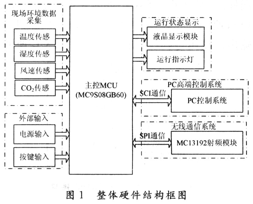

2.2.2 Interface circuit design of GB60 and MC13192 The interface circuit of GB60 and MC13192 is shown in Figure 3. GB60 and MC13192 mainly have 9 connection interfaces: 4 SPI communication interfaces, IRQ interrupt interface, 3 MC13192 control ports and MC13192 clock output pins. Among them, for 4-wire SPI, according to the reference manual, when used as the SPI host mode, and the SPI status and mode error flag (MODF) of the control register are effectively set to 1, the pin can be used as an I / O port alone. In this design, GB60 is the SPI host, which is directly used as the output port to control the CE enable signal of MC13192. 
The IRQ pin of MC13192 is connected to the IRQ pin of GB60, and all interrupt events generated on MC13192 are directly reflected to GB60. When the GB60 receives an external interrupt from the MC13192, it also needs to query its interrupt flag register to determine the interrupt event generated and make corresponding treatment.
Among the three control ports of GB60 to MC13192, the ATTN pin is used for MCU to wake up the MC13192 from low power consumption mode, and the RXTXEN pin is used to enable the MC13192 transceiver. In general, in order to reduce power consumption, the transceiver of the radio frequency chip is turned off, and it is only enabled when sending and receiving data, which can greatly reduce the power consumption of the radio frequency chip. When the RF chip works abnormally, the MCU can also reset the MC13192 through the RST pin.
The clock output pin CLKO of the MC13192 is directly connected to the EXTAL pin of the GB60, so that the GB60 no longer needs the support of an external crystal oscillator circuit, and the clock source from the MC13192 can be directly used. The clock source is programmable and can provide 8 different clock frequencies: 16 MHz, 8 MHz, 4 MHz, 2 MHz, 1 MHz, 62.5 kHz, 32.768 kHz and 16.393 kHz.
2.2.3 MC13192 wireless radio frequency communication module design The design of the radio frequency circuit is the most complicated part in the hardware design. This part has high requirements on the material of the PCB, the precision of the resistance and capacitance, and the wiring of the circuit. The selection of its parameters directly affects the quality of the RF circuit.
The design of the RF circuit is designed and developed with reference to the reference samples given by Freescale, Microchip and other companies.
(1) MC13192 support circuit design. The support circuit of MC13192 includes power supply circuit, filter circuit and crystal oscillator circuit, and its logical connection is shown in Figure 4. VBATT and VDDINT are power supply input pins. The normal working voltage of MC13192 is 2.0 ~ 3.6 V, and a 4.7μF voltage stabilizing capacitor must be connected. VDDA, VDDL01 and VDDL02 are rectified analog voltages and a 100 nF filter capacitor must be connected. VDD is the internally rectified digital voltage, which is connected to a 220 pF filter capacitor. VDDVCO powers the VCO circuit, and a 220 pF capacitor must also be connected. XTAL1 and XTAL2 are connected to a 16 MHz crystal oscillator dedicated to 2.4 GHz radio frequency circuit, and the bypass capacitor is 1O pF. 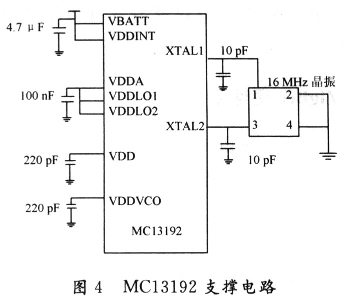
Figure 5 is a schematic diagram of the antenna circuit. RFIN- and RFIN + are receiving channels. Two 18 pF capacitors filter out high-frequency interference signals, while a 0.5 pF capacitor can prevent conjugate interference. PAO- and PAO + are transmission channels. These two pins are connected to VDDA to provide the necessary energy for the transmission channel. 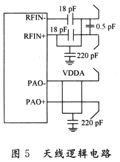
The basic testing process of the main modules of MT-ZigBee is as follows:
(1) Power module test. On the empty PCB circuit board, first solder the relevant components of the power module, and directly use a multimeter to measure the output point of the power supply after power-on to see if the required voltage value is obtained to ensure that other modules can work normally.
(2) Microcontroller part test. When the power module is working properly, you need to test whether the GB60 is working properly. The test for the MCU is mainly to communicate with the GB60 through the BDM writer to see if it can perform normal erase and write operations. If it does not work properly, you should first carefully check whether the MCU support circuit and the resistance and capacitance values ​​are correct, especially the crystal oscillator circuit. GB60 contains an internal clock source of 4 MHz and few peripheral circuits, so it is easier to debug and pass.
(3) MC13192 module test. For the test of the MC13192 RF module, it is mainly tested by reading and writing its internal registers and buffers.
(4) Test of other peripheral modules. Serial communication (SCI) is to realize basic sending and receiving through a PC; to test the small lamp module, the corresponding I / O port is set to a different value mainly through the MCU to see if the corresponding small lamp can be lit; to test the LCD module, see Whether to display the specified character on the LCD.
Model
Nominal Voltage
Nominal Capacity
Nominal impedance
Dimension
Charge-discharge standard
Approx Weight
(V)
(mAh)
(mQ)
Diameter
Height
Charge
Discharge
≈g
ICR10220
3.7
130
<150
10
22
0.5C-1C
0.5C-1C
4.1
ICR10440
3.7
350
<120
10
44
0.5C-1C
0.5C-1C
9
ICR14430
3.7
650
<100
13.8
42.8
0.5C-1C
0.5C-1C
17
ICR14500
3.7
900
<80
14
50
0.5C-1C
0.5C-1C
19.5
ICR17280
3.7
600
<100
16.3
28
0.5C-1C
0.5C-1C
15
ICR17335
3.7
700
<100
16.3
33.5
0.5C-1C
0.5C-1C
18
ICR18500
3.7
1400
<70
18.1
50
0.5C-1C
0.5C-1C
33
ICR18650
3.7
2000
<50
18.1
64.8
0.5C-1C
0.5C-1C
45
ICR18650P
3.7
2000
<40
18.1
65
0.5C-1C
3C-5C
45
ICR18650P
3.7
2200
<40
18.1
65
0.5C-1C
3C-5C
45
ICR18650
3.7
2600
<70
18.1
64.8
0.5C-1C
0.5C-1C
45
ICR26650
3.7
3500
<30
26
65.5
0.5C-1C
0.5C-1C
85
ICR26650P
3.7
5000
<30
26
65.5
0.5C-1C
0.5C-1C
85
ICR18650P
3.7
1500
<15
18.1
64.8
1C
10C-15C
47
ICR26650P
3.7
2200
<15
26
64.8
1C
10C-15C
64
IFR14430E
3.2
400
<115
13.8
43
0.5C-1C
0.5C-1C
15
IFR14500E
3.2
400
<95
13.8
50.2
0.5C-1C
0.5C-1C
15.5
IFR14500E
3.2
650
<80
13.8
50.2
0.5C-1C
0.5C-1C
17.8
IFR18500E
3.2
600
<80
18
50
0.5C-1C
0.5C-1C
19.5
IFR18500E
3.2
1200
<80
18
64.8
0.5C-1C
0.5C-1C
30.4
IFR18650E
3.2
1500
<65
18
64.8
0.5C-1C
0.5C-1C
40.5
IFR18650E
3.2
1700
<80
18
65.3
0.5C-1C
0.5C-1C
41.2
IFR26650E
3.2
3400
<20
26
65.3
0.5C-1C
0.5C-1C
87
IFR18650P
3.2
1100
<20
18
65.3
1-3C
10-25C
40
IFR26650P
3.2
2400
<20
26
65.3
1-3C
10-25C
82
January 13, 2024