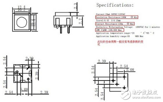
Today, two circuit design errors were written. The first one was caused by insufficient current gain. The circuit was triggered by other designers. After reading it, you can learn some knowledge. The main reason for the first error was that the designer incorrectly estimated the size of R1. The value of its design is too large, causing Ib to be too small. Here the equivalent model is converted as follows: The above model describes the model of input and output, and the formal calculation is divided into two parts. Solving the base current Ib Solving the collector current Ic Solve the amplification ratio The state of the triode can be obtained by this ratio. If it is in the linear region, the tube voltage drop Vce of the triode is varied, which causes a logic problem. The mistake is that a certain state cannot be identified. From a certain point of view, this is actually a level shifting problem, but it is isolated by a triode. Anyway, I personally do not recommend this connection, because too much restriction will cause the triode to undersaturate and enter the linear region. If the current limit is too small, it will fail under high frequency pulse surge. More and more dedicated interface circuits are now being used to handle such circuits, but there may be errors in direct short-to-ground or power supply (as specified in ISO 16750-2). So this problem is very tricky, the input part is actually a big problem, because you never want to be wrong when the signal enters. The well-designed circuit, due to the change in the on-resistance of the switch, causes the circuit to adjust to this parameter change, so the original effective signal is completely invalid in the MCU processing. The on-resistance value of the switch is mainly determined by the contact resistance of the switch contacts. The contact resistance value is the most basic parameter of the contact performance of the switch contact. The size of the contact resistance directly reflects the reliability of the contact contact of the switch. In fact, the contact resistance varies with the aging and wear of the switch. Foreign manufacturers have specified the worst on-resistance of the switch, which is generally not considered in China (and generally cannot be controlled too accurately). It should be noted that the on-resistance parameter in the switch we see now is generally measured by measuring the on-resistance of the switch. The more formal approach is to measure the on-resistance through aging experiments, estimate the degree of wear of the contacts and the contact of the loop to predict the life of the contacts. (aging experiment) Therefore, there is a need for sufficient margin when designing. There are two principles. The first one, Imagine the worst case you may encounter, and design down in this condition. In the second article, efforts are made to ensure that the module does not enter the worst condition mode. Zgar International (M) SDN BHD , https://www.szdisposable-vape.com


July 10, 2024