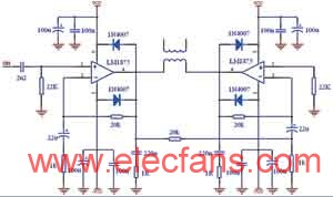
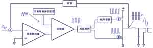
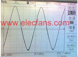
System Structure and Control Principle Boost + full-bridge inverter and output LC filter are one of the most commonly used topologies for high-power programmable AC power supplies. As shown in Figure 1, this is a two-stage non-isolated topology. The first stage is the boost stage, which is used to boost the module rectified voltage to the actual peak DC voltage (> 325V); the second stage is the inverter stage. It is used to convert the peak DC voltage into an AC voltage, and then obtain an AC output voltage of 50 Hz through the LC filter. The full-bridge inverter generally adopts the unipolar control mode, which is characterized in that the two power tubes of the high-frequency arm are complementarily switched with a high switching frequency to ensure an ideal sinusoidal output voltage waveform; the other two power tubes are compared. Low output voltage fundamental frequency operation, which greatly reduces switching losses. The full-bridge inverter is not always a low frequency (output fundamental frequency), the other bridge arm is always high frequency (carrier frequency), but is switched with half output voltage cycle, that is, the first half of the same bridge arm The cycle works at low frequencies, and the second half works at high frequencies, thus ensuring that the two bridge arm power tubes operate in an equilibrium state, improving system reliability. Although this circuit is more efficient, it needs to solve the isolation problem between input/output. Since the program-controlled AC power of the cable tester is small, if the above scheme is adopted, the volume is large and the control is complicated. Figure 1 boost + full bridge inverter If a monolithic integrated power amplifier component such as the LM1875 is used, the maximum output power can be up to 30W when powered by ±30V. The connection is similar to the TDA2030, with single and dual power connections and BTL connections. The BTL connection uses two LM1875s, which are connected into a bridge circuit. The circuit structure and parameters on both sides are identical. The integrated circuit on the right is controlled by the left integrated circuit through a negative feedback resistor, and vice versa. It can achieve higher output power. As shown in FIG. 2, the diode 1N4007 is used to prevent the output inductive load from generating an overvoltage and damaging the device. The amplification factor of the circuit can be determined by the feedback resistance from the output to the inverting input. Class A, Class B, Class AB and other power amplifiers are linear power amplifiers. The signal always stays in the amplification area. The output transistor acts as a linear regulator to adjust the output voltage. As a result, the efficiency is reduced and the output power is limited. Figure 2 BTL connection of LM1875 This design uses a Class D audio amplifier to form a programmable AC power supply. A high-purity sinusoidal AC voltage can be obtained by simply controlling the input amplitude of the audio amplifier. Figure 3 shows the block diagram of the developed program-controlled AC power system, and shows the waveform of each stage. Its main circuit consists of a Class D audio amplifier + half bridge and LC filter. Figure 3 Basic composition of the class D audio amplifier The main circuit design uses the IRS2092 from International Rectifier (IR) Class D audio amplifiers, which combines an error amplifier, PWM comparator, gate driver stage circuit and overload protection to provide greater design flexibility compared to the IRS20955. When powered by ±100V, the maximum output power is up to 500W and the operating frequency is up to 800kHz. As shown in Figure 4, it includes a pulse width modulator, two output MOSFETs, and a low pass filter for recovering the amplified audio signal. Since the output of the 500V sine wave is rms, there is a low frequency step-up transformer at the output. The audio input signal is compared with the triangular wave generated by the internal oscillator to obtain a PWM signal. The duty cycle of the square wave is proportional to the input signal level. When there is no input signal, the duty cycle of the output waveform is 50%. Figure 5 shows the PWM output waveform generated at different input signal levels. Figure 4 program-controlled AC power main circuit The key technology design program-controlled AC power supply requires 0~5V program-controlled DC level input corresponding to AC 0~500V (effective value) output. The maximum 500V sine wave output can be achieved by changing the amplitude of the sine wave input of the Class D audio amplifier. However, it is first necessary to solve the problem of how the 0~5V program-controlled DC level is converted into a sine wave input of a Class D audio amplifier. Figure 5 PWM output waveform Figure 6 Programmable diagram of the sine wave reference signal Figure 7 sinusoidal voltage output waveform Experimental results Using the above main circuit structure and control method, a program-controlled power supply prototype with 0~5V DC level input corresponding to 0~500V (effective value) AC output was developed. The fixed frequency is 50Hz, the output current is 5mA, the linearity is ≤1%, and the response is Time ≤ 50ms, output overcurrent protection. The 5V program-controlled sinusoidal voltage output waveform is shown in Figure 7, which satisfies the requirements of the cable tester program-controlled power supply.
This Solder Wire is with activated resin flux,It enjoys excellent weld ability,which can be divided into RA and RMA.which is made from extremely high purity raw materials.
Sn63/Pb37,Sn60/Pb40,Sn50/Pb50,Sn45/Pb55,Sn40/Pb60,Sn30/Pb70
Flux-Cored Solder Wire,Solder Welding Wire,Lead Free Solder Wire,Silver Solder Wire Shaoxing Tianlong Tin Materials Co.,Ltd. , http://www.tianlongspray.com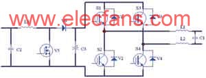
It is worth noting that the half-bridge Class D audio amplifier causes "bus voltage boost" because the energy can flow in both directions, which causes the bus capacitor to be charged. In a half-bridge topology, the power supply faces the energy returned from the amplifier and causes severe bus voltage fluctuations or damage, especially when the amplifier outputs low frequency signals to the load. Class D amplifiers differ from synchronous buck converters in that the reference signal is an ever-changing audio signal, the duty cycle is varied around 50%, the inductor current is bidirectional, and the two MOSFETs function the same. 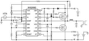
Using the BTL connection of the Class I audio amplifier IRS2092, a full bridge uses two half-bridge output stages and drives the load differentially. The full-bridge structure works by switching the conduction path of the load, so the load current can flow in both directions without the need for a negative supply or a DC-blocking capacitor. At the same supply voltage, the theoretical maximum output power is four times that of a half-bridge amplifier. It can be applied to AC/AC conversion power supplies with higher output power.
The CD4051 is an 8-channel digitally controlled analog switch with three binary control inputs A, B, C and INH inputs, which is equivalent to a single-pole, eight-throw switch. Which channel is switched on, the input 3-bit address code A, B, C to decide. INH is the disable terminal. When INH=1, each channel is not connected. In addition, the CD4051 is also equipped with a power supply terminal VEE for use as a level shift, so that the digital signal provided by the CMOS circuit can directly control the multiplex switch under a single power supply condition, and the multiplex switch It can transmit AC signals with peak-to-peak value up to 15V. For example, if the power supply of the analog switch is VDD=+5V, VSS=0V, when VEE=-5V, as long as the digital control signal of 0~5V is applied to the analog switch, the amplitude range can be controlled from -5V to +5V. Analog signal. 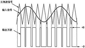
When designing, first consider how to generate a fixed-amplitude sine wave reference signal as an analog input to the CD4051. There are many ways to generate a sine wave reference signal. A good sinusoidal waveform can be obtained by the Wenner oscillator. The square wave output from the comparator can be obtained by the integrator to obtain a triangular wave, and then the differential amplifier or the low-pass filter can be used. , to achieve the transformation of triangular waves to sine waves.
Followed by the high-precision sine wave reference signal programming, the simplest method is to use the microprocessor for 12-channel A / D conversion, use these 12 channels to control the input end of the CD4051 A, B, C (INH = 0) , that is, 212=4096 states are generated. As shown in Fig. 6, switches D1 to D3 control the analog low bits and D4 control the high bits. By reasonably calculating R1a to R9d, 0 to 4096 states correspond to 0 to 5V programmable DC level inputs. It should be noted that the condition of the 4096th state is that when 12 channels are both 0 and the 4th CD4051 has INH=1, it outputs the sine wave analog maximum value. 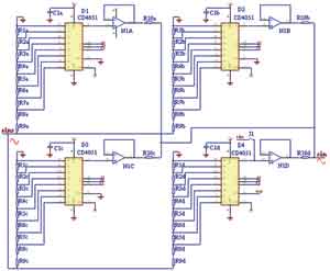
June 08, 2019