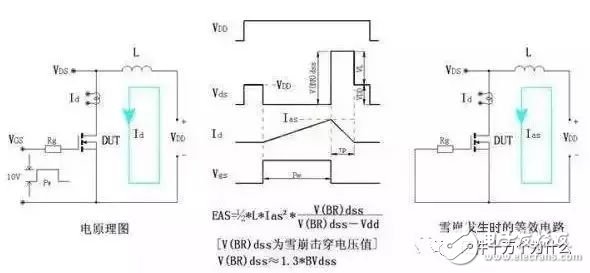
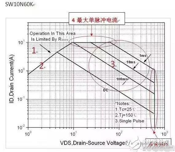
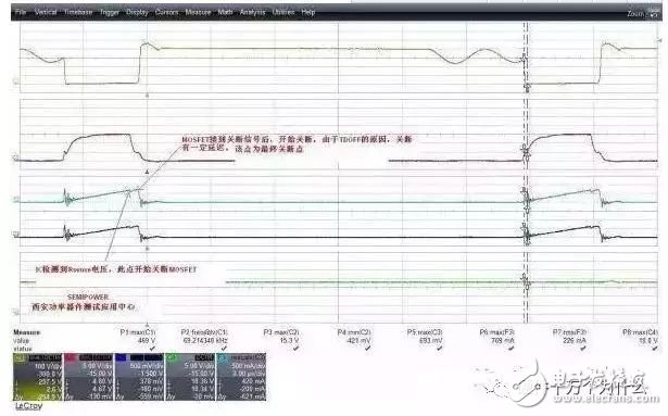
The MOS tube is a metal-oxide-semiconductor field effect transistor, or a metal-insulator-semiconductor. The source and drain of the MOS tube can be reversed. They are all N-type regions formed in the P-type backgate. In most cases, the two zones are the same, even if the two ends are reversed, it will not affect the performance of the device. Such devices are considered to be symmetrical. Currently in the market application, the number one is consumer electronic power adapter products. The second application area of ​​MOS tube is computer motherboard, NB, computer adapter, LCD display and other products. With the development of national conditions, computer motherboards, computer adapters, and LCD monitors have more demand for MOS tubes than consumer electronics. The phenomenon of the power adapter is gone. The third is in the field of network communication, industrial control, automotive electronics and power equipment. These products are also very demanding for MOS tubes, especially now that automotive electronics demand for MOS tubes is directly chasing consumer electronics. The following summarizes the following six points for the causes of MOS failure, and then analyzes the priorities of 1, 2: 1: Avalanche failure (voltage failure), which is often referred to as the BVdss voltage between the drain and the source exceeds the rated voltage of the MOSFET, and exceeds a certain capacity to cause the MOSFET to fail. 2: SOA failure (current failure), which exceeds the safe working area of ​​the MOSFET, causes the failure of the Id to exceed the device specification failure and the Id is too large, and the loss is too high. 3: Body diode failure: In the topology of bridges, LLCs, etc., which are useful for freewheeling of body diodes, failure due to damage to the body diode. 4: Resonant failure: In the process of parallel use, the gate and circuit parasitic parameters cause failure caused by oscillation. 5: Static failure: In the autumn and winter, the device fails due to static electricity of the human body and equipment. 6: Gate voltage failure: The gate gate oxide layer fails due to the abnormal voltage spike of the gate. Avalanche failure analysis (voltage failure) What is the avalanche failure? Simply put, the MOSFET is on the power board due to the bus voltage, transformer reflection voltage, leakage inductance spike voltage and other system voltages superimposed between the MOSFET drain source, resulting in a failure mode. In short, it is a common failure mode caused by the voltage of the MOSFET drain source exceeding its specified voltage value and reaching a certain energy limit. The picture below shows the equivalent schematic of the avalanche test. As a power supply engineer, you can easily understand. Maybe we often ask the device manufacturer to perform failure analysis on the MOSFET on our power board. Most manufacturers only give a conclusion such as EAS.EOS. So how do we distinguish whether it is avalanche failure? The following is an avalanche. Test the failed device map and we can compare it to determine if it is an avalanche failure. Preventive measures for avalanche failure Avalanche failure is ultimately a voltage failure, so prevent us from focusing on voltage. Specifically, it can be handled in the following manner. 1: Reasonable derating, the current derating in the industry generally selects 80%-95% derating, the specific situation is selected according to the company's warranty terms and circuit concerns. 2: Reasonable transformer reflection voltage. 3: Reasonable RCD and TVS absorption circuit design. 4: Large current wiring should adopt coarse and short layout structure as much as possible to minimize the parasitic inductance of the wiring. 5: Select a reasonable gate resistance Rg. 6: In high-power power supply, RC damping or Zener diode can be added as needed to absorb. SOA failure (current failure) Simply put the second point, SOA failure SOA failure refers to the abnormal mode in which the large current and voltage of the power supply are superimposed on the MOSFET at the same time, causing transient local heating. Or the chip and the heat sink and the package can not reach the heat balance in time to cause heat accumulation, and the continuous heat causes the temperature to exceed the thermal breakdown mode and the thermal breakdown mode. Refer to the picture below for the parameter limits for each line of SOA. 1: limited by maximum rated current and pulse current 2: Limited to RDSON at maximum temperature. 3: Limited by the maximum dissipated power of the device. 4: Limited by the maximum single pulse current. 5: breakdown voltage BVDSS restricted area The MOSFET on our power supply can effectively avoid the power failure caused by the MOSFET as long as the device is in the upper limit range. This is a solution to the failure of an atypical SOA that may not seem so straightforward due to the removal of aluminum. Preventive measures for SOA failure: 1: Ensure that all power constraints of the MOSFET are within the SOA limit line under worst-case conditions. 2: The OCP function must be precise and detailed. When designing the OCP point, engineers who may take 1.1-1.5 times the current margin are generally used, and then the RSENSE resistor is started according to the protection voltage of the IC such as 0.7V. Some experienced people will take into account the detection delay time and the actual impact of CISS on OCP. But at this time there is a more interesting parameter, that is, the Td(off) of the MOSFET. What effect does it have? Let's look at the FLYBACK current waveform below (the graph is not too clear, sorry, it is recommended to double-click to enlarge). As can be seen from the figure, when the current waveform is approaching the current spike, there is a fall. After this falling point, there is a rise time. The essence of this time is that the IC detects the overcurrent signal and turns off the MOSFET. The shutdown itself is also started, but due to the turn-off delay of the device itself, the current will have a secondary rise platform. If the secondary rise platform is too large, it is highly probable that magnetic saturation will occur when the transformer margin is insufficient. A current surge or current failure of a device specification. 3: Reasonable thermal design margin, this is not much to say, each company has its own derating specifications, strictly enforce it, and can not add radiators. Vent spacer,stator core vent spacer lamination,stator core vent spacer,vent plates Henan Yongrong Power Technology Co., Ltd , https://www.hnyongrongglobal.com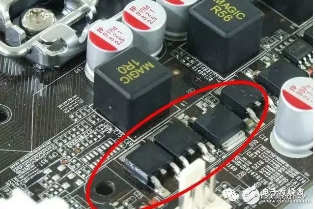

November 17, 2022