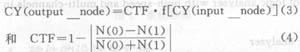
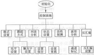
1 Introduction The test object of the logic analyzer is the digital information in the digital system [1]. In order to meet the detection requirements of the modern data domain, the logic analyzer should have a high sampling rate and enough input channels. Based on the concept of virtual instrument, this article mainly discusses the design principle and method of 400MHz/102 channel logic analyzer based on PC586, and focuses on the design of system control circuit and system software. 2 Virtual logic analyzer architecture Figure 1 is a functional block diagram of the overall structure of the 400MHz/102 channel virtual logic analyzer control and acquisition system in a PC environment, which mainly includes data acquisition, probe, trigger tracking, timing conversion and generation, and test interface. The input collection of the system is composed of 3 modules, each module has 32 data channels (additional 2 clock channels), using exactly the same functional structure. The third module adds functions such as clock input and output, and control. The main reason for adopting this structure is to avoid the problem of heat dissipation caused by the main acquisition board being too large and the components being too dense (due to more high-speed working devices), and the second is the flexible system structure, which can be selected according to the needs of 32, 64, 96 channels Configuration method. The control and management of the logic analyzer, data processing and data display are completed by an embedded computer. Therefore, the design of the system hardware mainly focuses on high-speed data capture and the interface with the microcomputer, while the software design mainly focuses on the system management, data post-processing and data display. Figure 1 Block diagram of 400MHz/102 channel virtual logic analyzer 3 system hardware design The high-speed data capture in the 400MHz/102-channel virtual logic analyzer is realized by the control circuit to complete trigger control and data access control, and the control circuit realizes the interface with the microcomputer at the same time. 3.1 Principles of Data Storage When doing state analysis, the logic analyzer works synchronously with the system under test. In order to make the state data stored in the memory consistent with the data flow of the system under test, it should meet: DATA*/FWEN=f(sclk,trw,dtc)*data(1) In formula (1), DATA is the data stored by the logic analyzer; /FWEN is the write enable control of the logic analyzer's main memory FIFO; sclk is the state (external) clock; trw is the trigger word; dtc is the data control; data is Data of the system under test. From formula (1), we know the following formula: DATA=data(2) The condition to be established is that the /FWEN signal and the sclk, trw, and dtc signals must comply with a strict relationship. According to the controllability theory in the design of digital system testability, using CAMFLOT[2] method (Computer Aided Measure For Logic Testability), there are: In formulas (3)~(4), CY is the degree of controllability, and its value ε(0,1); CTF is the controllable transfer factor; N(0), N(1) are all different inputs added to the circuit input Value, the total number of times "0" and "1" appear at the output of the circuit. From equation (3), when control signals such as sclk, trw, dtc, etc. are reliably set, the following can be calculated: CY(/FWEN)=1(5) That is, /FWEN is fully controllable, so that DATA=data is guaranteed. When doing timing analysis, the logic analyzer works asynchronously with the system under test. At this time, need to meet: DATA*/FWEN=f(trw)*data (6) At the same time, the sampling frequency is 5~10 times of the working frequency of the system under test, which can effectively store the data stream to be observed, and obtain sufficient observation range and satisfactory time resolution. 3.2 The realization principle of trigger control Knowing from the principle of data storage, one of the keys to the correct storage of FIFO data in logic analyzers is the control of trw, that is, triggering control such as start, stop, delay (clock, event), random, sequence, combination and limit through trigger recognition . Using the bit memory mapping method, using high-speed EPLD [3] combined with trigger memory, the designed block diagram for the realization of trigger control is shown in Figure 2. Figure 2 Block diagram of the realization of trigger control 4 System software design Using the image interface operating system Windows and the Windows-based visual programming platform C++++Builder, the software is composed of 15 windows plus 5 unit files, and the relationship between the main windows is shown in Figure 3. Figure 3 The windows of the system software and their relationships 5 concluding remarks The logic analyzer has a complex structure and high technical requirements. The design ideas and methods based on the concept of virtual instrument described in this article greatly simplify the hardware circuit due to the softening of some hardware functions. At the same time, EPLD devices are used, which reduces the cost of the instrument and improves the reliability and performance of the instrument. Easy to expand. The 400MHz/102 channel logic analyzer passed the technical appraisal hosted by the Military Industry Research Bureau of the Ministry of Information Industry on December 28, 2000. Shenzhen GEME electronics Co,.Ltd , https://www.gemesz.com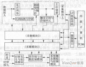
In Figure 2, D0~Dmk-1 are measured data. The trigger RAM data bit width is n, the address width is k, and the number is m, so the width of the observable data stream is m·k. When k≥n, the maximum sequence trigger or combination trigger recognition level L is:
L≦2n-1(7) 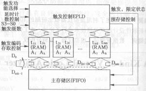
May 10, 2023