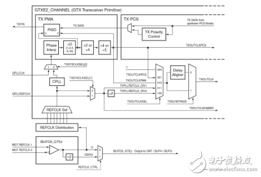
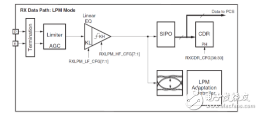
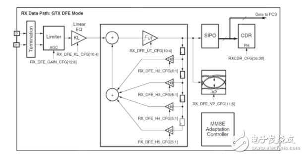
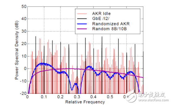
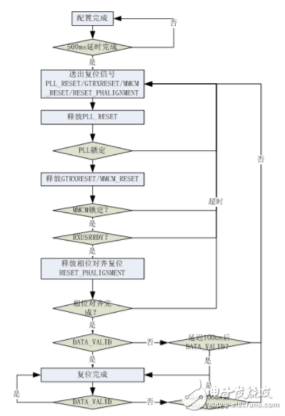
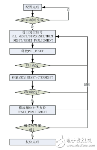
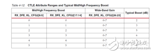
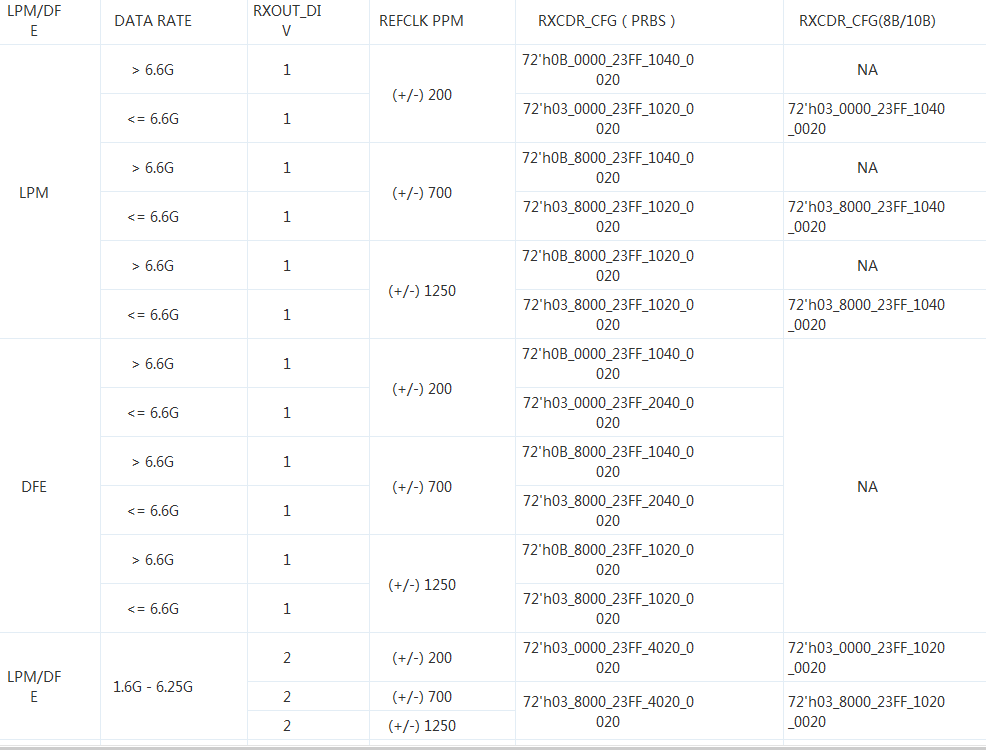
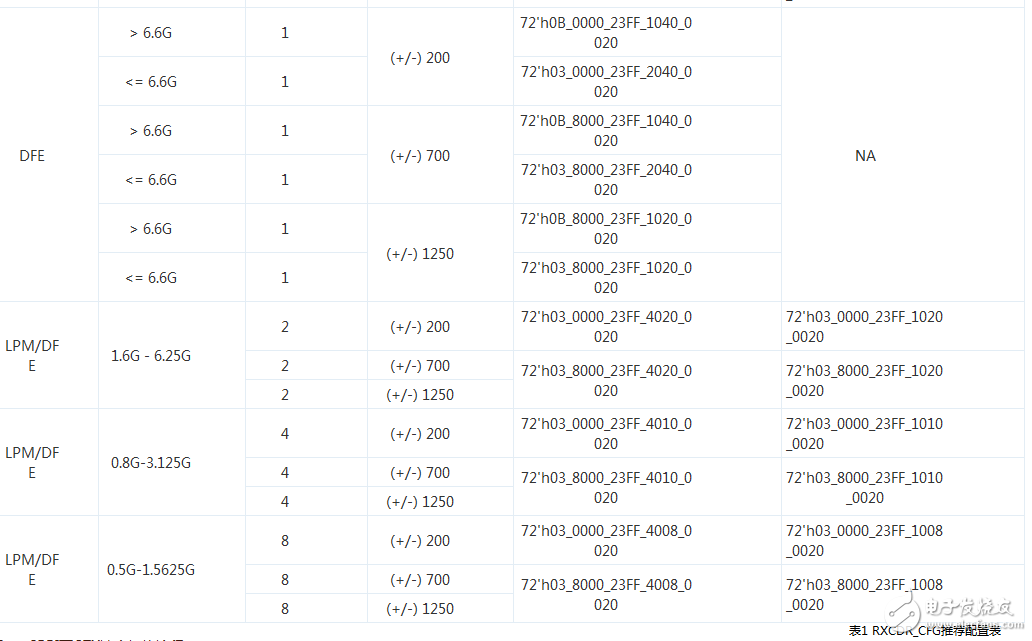
The GTX of the Kintex7 series, with its excellent performance and power consumption performance, has become the star of the industry's FPGA selection. Due to its good DFE performance, it can provide up to 12.5Gbps backplane capability and can support reliable transmission over channels with up to 30dB insertion loss. Among the numerous SERDES applications, some applications are special, that is, they need to dynamically switch the link rate of GTX during the actual operation process. For example, the CRPI interface in wireless needs to support many speeds such as 9.8G, 4.9G, and 2.4G at the same time. So how can we reliably switch between rates? This article is the subject of this, hoping to give full play to the advantages of GTX. The structure of Kintex7's SERDES is shown in Figure 1. Figure 1 Kintex7 GTX block diagram Taking the sending direction as an example, refer to the clock distribution diagram of the sending direction in FIG. 2 : Figure 2 GTX transmit direction clock distribution When Kintex7 performs link rate switching, there are mainly the following methods: 1) Switch QPLL/CPLL reference clock source; 2) Modify the QPLL/CPLL parameter settings via the DRP interface 3) Switch the QPLL/CPLL to provide the link clock; 4) Adjust the PMA's frequency division factor. Inside the GTX, there are 2 operating modes: LPM mode and DFE mode. LPM (Low Power Mode) mode is a low power mode, which mainly supports low insertion loss channels, a link rate of "11.2G, and a channel insertion loss of 12 dB or less. In LPM mode, both CTLE and baseline wander cancellaTIon are fully automatic and do not require manual adjustment. The structure of the LPM model is as follows: Figure 3 GTX structure diagram in LPM mode DFE mode provides better channel compensation, it can support link rates up to 12.5G, and performs well in scenarios where the channel insertion loss is greater than 8dB. DFE is different from CTLE in that it does not amplify noise and crosstalk and can correct reflections caused by channel discontinuities. It can automatically use AGC, CTLE, DFE and baseline wander cancellaTIon to complete channel compensation. It also supports CTLE manual mode. The structure of GTX in DFE mode is shown in Figure 4. Why does 8B/10B be introduced separately? This is mainly due to the 8B/10B-encoded system, which basically sends fixed-pattern data when the system is idle, such as /I1/ and /I2/ defined in 802.3. The data of a fixed pattern has a relatively discrete spectrum and there are too many glitches, which is not conducive to EMI and is not conducive to DFE for compensation tracking. In general, when the link rate is 5 Gbps, simply using 8B/10B encoding is not suitable. Many protocols typically use scrambling instead of scrambling or scrambling the data before 8B/10B encoding. In practical applications, fast FFT analysis can be performed on an oscilloscope to obtain its spectral characteristics. If there are more spectral glitches, then you need to consider improving the signal spectrum at the transmitter. Figure 5 shows the spectrum of different modes under 8B/10B coding. From the figure, it can be seen that the AKR IDLE and /I2/ under the GbE that transmit the fixed sequence have many spectral glitches and are not suitable for the DFE work. Figure 5 Spectrogram If you instantiate GTX with ISE 14.4, the IP version of GTX should be 2.4. In this version of the example code, full consideration is given to the GTX reset flow. It can be used as a template for everyone to design GTX reset processing. A general principle of the reset sequence is: from the PLL, to the PMA, then to the PCS, then to the user logic, in order. It should be noted that the reset of the GTX is started with a unified GTRXRESET/GTTXRESET and the reset mode is configured as a sequenTIal reset. In the receive direction, the reset flow is roughly: Figure 7 GTX Receive Direction Reset Flowchart In the sending direction, the reset process is roughly: Figure 8 GTX send direction reset flow chart The configuration of GTX needs to focus on: 1) AGC; 2) CTLE; 3) RXCDR_CFG; 4) Pre-emphasis in the sending direction. This article focuses on the first three items. In the LPM mode, both AGC and CTLE are fully automatic modes. It also provides HOLD, OVERRIDE ports for controlling, such as {RXOSHOLD, RXOSOVRDEN}, {RXLPMLFHOLD, RXLPMLFKLOVRDEN}, {RXLPMHFHOLD, RXLPMHFOVRDEN}. In the DFE mode, HOLD and OVERRIDE ports are also provided for controlling various attributes. It is also divided into CTLE Auto mode and CTLE Manual mode. The CTLE Auto mode can be enabled by modifying the following attributes of the DRP interface. RX_BIAS_CFG[5:4] = 2'b11 RX_DFE_KL_CFG2[26:23] = 4'b0111 RX_DFE_LPM_CFG[5:2] = 4'b0010 In the CTLE Manual mode, by modifying the RX_DFE_KL_CFG2 attribute through the DRP interface, the frequency response curve of the CTLE can be adjusted to obtain a value suitable for the channel. Figure 9 CTLE settings in DFE mode In addition to the above configuration, the RXCDR_CFG attribute is also affecting GTX performance, and it can only be modified through the DRP interface. The specific recommended configuration values ​​are shown in Table 1. CPRI is generally divided into the following working link rates: 1) 2.4576 Gbps 2) 3.072 Gbps 3) 4.9152 Gbps 4) 6.144 Gbps 5) 9.8304 Gbps In practical applications, if the highest speed needs to support 9.8304 Gbps, QPLL must be enabled. Since each Quad has only one QPLL, if the four GTXs in the Quad are to individually adjust the link rate, the QPLL can only work at 9.8304 Gbps. The following is divided into 2 situations for discussion: a) The supported rates have a double speed relationship; You only need to modify the RXOUT_DIV and TXOUT_DIV attributes of the PMA section, or the RXRATE and TXRATE ports, and the QPLL only works at 9.8304 Gbps. b) The supported rate has no double speed relationship. Except for 9.8304 Gbps and other rates that have a double speed relationship with 9.8304 Gbps, other rates are supported by the CPLL. You can talk about PowerDown when the CPLL is not in use. Regardless of which configuration scenario above, the most basic rate switching process will not be much different. The switching process should generally be as follows: Step1: Update related attributes through DRP interface: RXCDR_CFG, the value specifically refers to Table 1 RX_BIAS_CFG RX_DFE_KL_CFG2, the value of specific reference Figure 9 RX_DFE_LPM_CFG RXOUTDIV TXOUTDIV Step2: Reset GTX, refer to GTX reset process. It is worth noting that the optimal values ​​of RXCDR_CFG and RX_DFE_KL_CFG2 are different due to inconsistent channel performance at different link rates. Therefore, when switching the rate, the optimal value must be configured to GTX through the DRP interface. When switching LPM mode and DFE mode, you must also perform a full reset from the PMA. The USB 3.2 specification absorbed all prior 3.x specifications. USB 3.2 identifies three transfer rates – 20Gbps, 10Gbps, and 5Gbps. Usb 3.2 Cable,Usb Type-C Cable,5Gbps Usb Type-C Cable,10Gbps Usb Type-C Cable UCOAX , https://www.jsucoax.com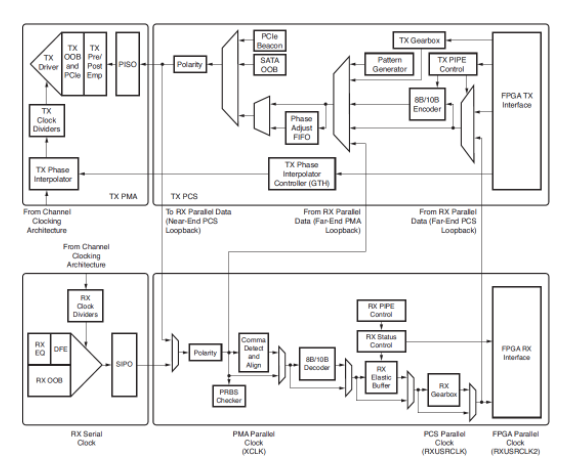
Key characteristics of the USB 3.2 specification include:
Defines multi-lane operation for new USB 3.2 hosts and devices, allowing for up to two lanes of 10Gbps operation to realize a 20Gbps data transfer rate, without sacrificing cable length
Delivers compelling performance boosts to meet requirements for demanding USB storage, display, and docking applications
Continued use of existing USB physical layer data rates and encoding techniques
Minor update to hub specification to address increased performance and assure seamless transitions between single and two-lane operation
Improved data encoding for more efficient data transfer leading to higher through-put and improved I/O power efficiency
Backwards compatible with all existing USB products; will operate at lowest common speed capability
May 30, 2023