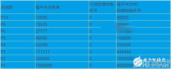
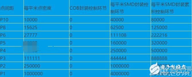
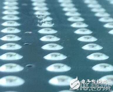
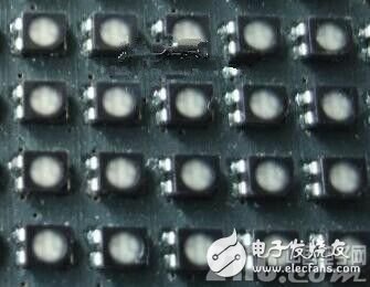
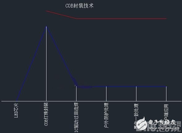
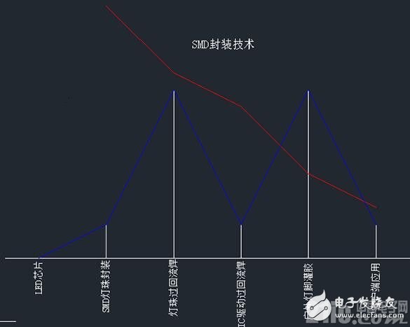
COB packaging has gradually matured in the field of LED display applications, especially in the field of outdoor small pitches with its unique technical advantages. Especially in the past two years, with the improvement of production technology and production process, COB packaging technology has made qualitative breakthroughs. Some factors that restricted development in the past have also been solved in the process of technological innovation. So, what is the advantage of COB packaging technology? How is it different from traditional SMD packaging? Will it replace SMD and become the mainstream of LED display in the future? Generally speaking, whether a certain packaging technology has vitality is to see its tail (customer application side) from the head of the industry chain (LED chip). Evaluation through comprehensive analysis. Among them, the final judgment of a certain packaging technology must come from the client application, not a link in the industry chain. This article will analyze and compare the two packaging forms of COB and SMD to discuss the best packaging form in the field of LED display. In general, COB packaging and SMD packaging stand on the same starting line in the selection of LED chips, and then choose different technical routes. 1. Different technologies COB packaging is to directly fix the LED chip on the pad of the lamp bead lamp position of the PCB board with conductive glue and insulating glue, and then solder the conduction performance of the LED chip. After the test is completed, it is encapsulated with epoxy resin. The SMD package is to fix the LED chip on the pad of the lamp bead bracket with conductive glue and insulating glue, and then soldered with the same conduction performance as the COB package. The process of cutting and taping and transporting to the screen factory. 2. Comparison of advantages and disadvantages There is no doubt that SMD packaging factories can produce high-quality lamp beads, but the production process is too much, and the cost will be relatively high. It will also increase the cost of transportation, material storage and quality control from the lamp bead packaging plant to the screen plant. And SMD believes that COB packaging technology is too complicated, and the product's one-time pass rate is not well controlled by a single lamp, or even an insurmountable obstacle. The failure point cannot be repaired and the yield is low. In fact, the current equipment technology and quality control level of COB packaging, 0.5K integrated technology can achieve a pass rate of about 70%, 1K integrated technology can reach about 50%, 2K integrated technology can make the This index reached about 30%. Even if there is a module that fails the one-time pass rate detection, the defective points of the whole board are 1-5 points. There are few modules with more than 5 defective points. Testing and rework before sealing is to make the finished product pass rate It reaches about 90% -95%. With the advancement of technology and accumulation of experience, this indicator will continue to increase. At the same time, we also have the technology of repairing the defective points one by one after sealing. 3. Technical analysis and evaluation Technical Analysis Evaluation Form Analysis and evaluation instructions: Technical difficulty: SMD packaging: Obviously, this single lamp bead monolithic packaging technology has accumulated many years of practical experience. Everyone has unique skills and scale, and the technology is mature. It is relatively easy to implement. COB packaging: It is a new packaging technology with multiple lamp beads integration. In the process of practice, a lot of technical experience in production equipment, production process equipment, test and inspection means, etc. is accumulated and verified in continuous innovation practice, and the technical threshold is high High difficulty. The biggest difficulty currently facing is how to improve the product's one-pass rate. COB packaging is facing a technological peak, but it is not insurmountable, but it is relatively difficult to achieve. Factory failure rate control level: Both COB and SMD packaging can be controlled very well, and can guarantee zero failure rate when handed over to customers. Cost Control: Theoretically speaking, the cost control of COB in this link should be slightly better, but the current production capacity is limited, and scale has not yet been formed, so for the time being, SMD has an advantage. Reliability risks: The four-corner or hexagonal brackets used in SMD packaging have brought technical difficulties and reliability risks to the subsequent production process. For example, the over-reflow soldering process of the lamp bead surface needs to solve the problem of a large number of bracket pin soldering yields. If the SMD is to be applied outdoors, the outdoor protection yield rate of the support pins must be solved. The COB technology is due to the omission of this bracket, and there will be no more technical difficulties and reliability risks in the subsequent production links. There are only two technical hills: one is how to ensure that there is no failure point on the lamp bead surface when the IC driver chip surface is reflowed, and the other is how to solve the problem of module ink color consistency. Over-reflow soldering process of lamp bead surface 1. Technical differences Since there is no bracket for COB packaging, this process does not exist. SMD packaging is to purchase the lamp beads of the SMD packaging factory from the display factory, and then process the patch to the PCB board. 2. Some questions A. Competition issues This link is different from the packaging link. The packaging link is in the middle of the industry chain. There are only a handful of enterprises, and there will be a certain profit margin. The screen factory link is downstream in the SMD industry chain. There are many companies with relatively low technical thresholds, fierce competition, thin profits, and great survival pressure. Among the many screen factory companies, the companies listed through financing occupy the main position by virtue of their financial strength, brand advantages and foreign market channel advantages. Other small and medium-sized enterprises can only be big waves if they do not have differentiated products. The uneven development level of enterprises will inevitably lead to an increase in the differentiation of product quality. What will companies do in such an environment and how? If you want to do a good job in this link and minimize the problem of product reliability decline, the technology used seems simple, but it is not. The following three factors deserve everyone's attention? PCB board design quality, material, manufacturing process, process and storage quality control level. SMT equipment accuracy and SMT production process quality control level. Faced with market competition, managers' cost awareness and quality awareness. We believe that competition to reduce raw material quality and sacrifice product quality will have disastrous consequences for the industry chain. B. Product cost COB packaging does not have this process, and the cost in this link is always zero. As the density of product points increases in SMD packaging, the difficulty of placement technology increases and the cost of the product increases. And the higher the dot density, the more the cost increases, and the relationship is non-linear and accelerates growth. C. Reliability issues COB packaging does not have this process, and there is no problem of reliability reduction in this link. Since there are generally 4 solder pins for each bracket in SMD packaging, there must be a problem of reduced reliability at this stage. This is determined by reliability theory. According to the principle of reliability, the fewer the control links of a product, the higher the reliability. Please see the table below: Comparison of the quality control of COB packaging and SMD packaging in the reflow soldering process of module lamp From the table, we can clearly see the fact that the COB package with the dot pitch becomes smaller and the dot density increases, the control link of its lamp bead surface is always 0, and the SMD package with the dot pitch becomes smaller With the increase in dot density, its control link per square meter will increase by a factor of four with the corresponding increase in dot density per square meter. D. The problem of lamp bead failure caused by reflow oven temperature SMD lamp bead devices usually require a temperature of about 240 degrees when over-reflow soldering, and lead-free soldering even needs to reach a furnace temperature of 260-280 degrees. There are two possibilities for the lamp bead device to pass through the reflow soldering machine. One kind of failure is the hidden danger of cracking and fragmentation of LED chips under the action of high temperature: LED chips are like humans, and there are normal and abnormal individual differences. When weak and disabled individuals pass the high temperature, they will not stand the test Kind of problem. If it fails immediately after the furnace, the problem is not big, just replace it. The fatal thing is that this kind of hidden trouble can still light up after passing the furnace, and it can also pass the aging test, after transportation vibration, or after a period of use at the client, it will fail. Another type of failure is the failure to pull off the LED chip solder wire. E. Friendly issues in the application process COB encapsulated lamp beads are fixed on the PCB board by epoxy resin. The affinity of epoxy resin glue and PCB board is extremely strong, and it has the following physical properties: Compressive strength: 8.4kg / mm² Shear strength: 4.2kg / mm² Impact resistance: 6.8kg * cm / cm² Hardness: Shore D 84 Therefore, it is not afraid of static electricity, knocking, impact, bending deformation, wear resistance and easy cleaning. Therefore, the contact with people is very friendly, not spoiled and durable. The SMD package lamp beads are soldered to the PCB board through the pins of the bracket, and the physical strength test performance is not high. Fear of touch, fear of static electricity failure caused by touch, and not friendly to people. 3. Analysis and evaluation In this aspect, the advantages of COB packaging have already emerged. There is no vicious competitive environment, and there are no cost and reliability problems. Therefore, it is not only the concept of physical space that COB is easy to achieve a small pitch, but also the advantages of cost and reliability. SMD packaging is facing a breakthrough in how to improve the soldering yield rate of bracket pins in this link, which requires a lot of manpower, material resources and financial resources. And as the dot density becomes denser, the cost and reliability issues become more and more prominent. 1. Technical differences COB packaging has been plagued by the problem of ink color consistency for a long time, and this problem can now be solved technically. SMD packaging uses the mask technology to solve the ink color problem. 2. Analysis and evaluation The cost of the two packages to solve the ink color problem is roughly the same, and neither will have the effect of reduced product reliability. 1. Technical differences COB-encapsulated LED wicks have been encapsulated with epoxy resin, and there are no exposed solder legs. The problems to be solved by outdoor protection are only PCB board protection treatment and waterproof structure design. The technology is very simple. A. PCB protection There are two protection levels. General outdoor application level (such as rental and fixed installation): three anti-paint treatment process. High and low temperature, humidity, salt spray environment application level: nano coating + anti-UV + three anti-paint treatment process. B. Waterproof structure design After the COB module is treated with double-sided outdoor protection, both sides are not afraid of water. In order to make the power supply, drive card and drive IC in the box work in a good environment and can work longer, the module structure design uses a fully sealed design for outdoor protection. The COB module drive IC has It is sealed with a silicone seal ring. There is also a heat-dissipating aluminum plate under the seal ring. The aluminum plate is embedded and fixed in the plastic parts kit. There is also a layer of silicone seal ring between the kit and the box body to ensure that no water will enter the module and the box body. SMD packaging requires that the SMD device's support patch pins be encapsulated and protected, especially to the density above P4, and the technical difficulty is quite large. 2. Facing problems A. Competition issues Since COB packaging has not yet formed a large-scale production capacity, it is currently at the P8-P10 level and has not yet formed a cost advantage. At present, it is only in the sports venues and rental markets that it needs to break down the outdoor display and high and low temperature, humidity, salt spray application environment and other breakdown The special application market has application advantages. At the P5-P6 level, the cost is comparable to SMD. In P4-P3 and even denser grades of pure outdoor applications, the cost will have an absolute advantage. Once the capacity is formed in the future, COB packaging will have a price advantage at all point density levels, and there is currently no competition between COB peers. SMD faces the competition between peers as mentioned above, so the quality of the bracket is very important. To save costs and reduce the height of the bracket, it will increase the difficulty of grouting technology and reduce the yield rate of grouting. Not only does it not save costs, but it will also cause reliability Reduce and increase the processing cost of gluing. B. Product cost The cost of this process of COB packaging is basically calculated according to the outdoor processing cost per square meter, and has little to do with the increase in point density. The cost of SMD package outdoor protection treatment increases with the increase in product point density and the difficulty of potting technology. And the denser the dot density, the more the cost increases, showing a non-linear and accelerated growth relationship. C. Reliability issues The surface of the COB package lamp has been encapsulated with epoxy resin. In this process, there are no exposed chips and pins that need to be processed. You only need to protect the PCB board for outdoor protection. There is basically no problem of reduced reliability. There are 4 solder pins for each bracket of the lamp surface of the SMD package, which needs to be encapsulated and encapsulated. Therefore, there is a yield rate index of the encapsulated and encapsulated pins of the bracket. As with the reflow soldering link, there is a problem of reliability reduction caused by the support pins in this link. According to the principle of reliability, the fewer the control links of a product, the higher the reliability. Please see the table below: Comparison of the quality control of COB packaging and SMD packaging for outdoor protection technology of module lamp bead surface From the table, we can clearly see the fact that the COB package with the dot pitch becomes smaller and the dot density increases, the control link of its lamp bead surface is still 0, while the SMD package with the dot pitch becomes smaller With the increase in dot density, its control link will continue to increase by a factor of four with the corresponding increase in dot density. Cumulative control link refers to the accumulation of SMD reflow soldering process control link and potting process control link. As can be seen from the data in the table, this value increases 8-fold with the increase in point density. In an over-competitive environment, the height of the outdoor SMD lamp bead pin has been continuously reduced, which makes the implementation of this technology more difficult. How to fill the glue in such a small height space, cover all the pins, and control the level of the module is indeed a very difficult technology. D. Outdoor protective treatment The surface of the lamp beads in the COB package is a hemispherical curve. All the devices on the lamp surface are encapsulated by epoxy resin. There are no device pins exposed on the outside, and the curve is too smooth and no corners. If spraying technology is used, no matter whether it is the principle of electrostatic adsorption or the principle of vacuum vapor deposition, it can be processed without dead ends. Therefore, no matter whether it is used indoors, outdoors, or in the harsh high and low temperature, humidity, and salt fog environments, there is no worry about the failure of the lamp beads caused by the oxidation of the device pins. The COB package PCB board must be immersed in gold, which ensures that the device is not easily oxidized during the entire process, thereby ensuring that there is no hidden danger of device pin oxidation when the PCB board is sprayed on both sides. SMD encapsulated lamp beads will have a lot of raised tetragons with sharp edges and corners. The pins of the bracket exposed on the surface of the lamp bead need to be protected by outdoor protection. If the indoor lamp beads want to be improved to be used in semi-outdoor, especially in the humid and salt fog environment, it must be sprayed. If the PCB board adopts the tin-spray manufacturing process, the device pins are prone to oxidation hazards during the manufacturing process, and then spraying will not be ideal. There is a blind spot in the shadow area under the lamp bead abdomen. 3. Analysis and evaluation In this aspect, the advantages of COB packaging have once again appeared, and there is no problem of reduced reliability. At present, outdoor technology has broken through to P3.0 level. SMD packaging continues to face the technical problem of how to improve the yield rate of the outdoor protection grouting of the support pins. For small outdoor pitches, the technology is more difficult and requires a lot of manpower, material and financial resources to break through this technology. And as dot density becomes higher, cost and reliability issues become more prominent. The two packages finally came to the end customer through different technical routes, and their experience is the most powerful. Theoretical analysis needs to be evaluated through their practical application. With the continuous increase of actual cases of COB packaged display screens and the continuous expansion of special application fields, the market will definitely make analysis and selection of these two packaging technologies. The power of this choice comes from the market, from the very end of the industry chain. Here we only give the reliability data of COB outdoor products after one year of use on the terminal client (except for the cottage version of COB products): Full color screen dot failure rate: less than five hundred thousandths Single and double color screen dot failure rate: less than 8 parts per million Conclusion: To sum up the detailed comparative analysis of each link, use the following two figures to make a summary of the two technical styles in the LED display industry industry chain. COB packaging technology: From the beginning of packaging to the completion of display manufacturing, COB packaging technology integrates the middle and downstream links of the LED display industry chain, and all production is completed in one factory. This type of production organization is simple, the process is compact, the production efficiency is higher, and it is more conducive to the fully automated production layout. This form of organization is also more conducive to quality control throughout the product process. This form of organization is still an organic whole. At the product development stage, we must consider the problems that may be encountered in each production link, comprehensively evaluate and formulate the technical implementation plan. This form of organization can also better assume quality responsibility for end customers. From the perspective of the ease of technical implementation and the impact on product reliability in the entire production process, as can be seen from the following figure, the white abscissa represents the main process link in the industrial chain The white bar on the node indicates the technical difficulty. The red line in the upper part of the figure represents the product reliability curve from the packaging link to the client application link. The blue line represents the technical difficulty curve at different links in the industrial chain. It can be seen from the figure that COB packaging is facing only one technological peak on the road of multi-lamp bead integration packaging technology in the field of LED display, which appears in the lamp bead packaging link. And this technology is not insurmountable, but not everyone can climb through. It is an embodiment of comprehensive technology. It requires countless failures and lessons learned. It takes years of technology accumulation and precipitation. It needs firmness, down-to-earth, A craftsman who is not afraid of difficulties and has the courage to innovate. Once this technical peak is crossed, like the carp jumping the dragon gate, the road behind the mountain will be a flat horse. There are no more technical difficulties in the entire production process. From the red product reliability curve, it can be seen that once the lamp beads are sealed in the COB package, the subsequent production link has little effect on its reliability. After one year of application on the client, the reliability index is almost the same as the packaging time. SMD packaging technology: Packaging companies and display companies in the SMD display industry chain are two types of independent companies, and industrial profits are shared by these two types of companies. Although the cake is large, there are many enterprises, fierce competition and thin profits. This type of production organization is complicated, it will waste a part of industry profits and efficiency, and product quality control is relatively difficult. Due to the independence of the packaging link and the display panel link, it is difficult to effectively cooperate with each other to cope with technical difficulties in the production process. Once the quality problems of the products used by the end customers are involved, there are many links involved, and it is difficult to blame. From the perspective of the difficulty of technical implementation in the entire production process and the impact on product reliability, the color and meaning of the curve in the figure below are the same as the previous figure. It can be seen from the figure that there is a double hump-shaped technology peak in the SMD display packaging industry chain. Both of these technical difficulties appear in the screen factory link, and the packaging link is relatively difficult because the technology is mature and stable. Therefore, the technical difficulty of SMD display screens will certainly exceed the difficulty of COB packaging technology. The deterioration of the competitive environment and the imbalance of profit distribution affect the trend of the product reliability red line from the packaging factory. Although the red line of each factory has high and low, but their downward trend when reaching the client application is Doubt is determined by reliability theory. This is the real reason why the customer's application-end perception of product reliability is inconsistent with the packaging factory's factory standards. Therefore, the reliability of SMD products is mainly determined by the screen factory. In the future, in the display field, which packaging method has more vitality, I believe that the end user will make the right choice. Providing customers with cost-effective display products is the direction of COB packaging efforts. COB packaging will make important contributions to the development of the industry in terms of product reliability and price civilianization. VEIIK Vape is so convenient, portable, and small volume, you just need to take them out of your pocket and take a puff, feel the cloud veiik vape disposable,veiik vape pen,veiik e cigarette,veiik vape kit,veiik disposable vaporizer Ningbo Autrends International Trade Co.,Ltd. , https://www.vapee-cigarettes.com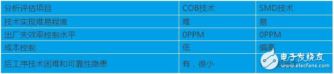

of smoke, and the fragrance of fruit surrounding you. It's so great.
We are the distributor of the VEIIK Vape brand, we sell veiik e cigarette, veiik vape pen, veiik disposable vaporizer, and so on.
We are also China's leading manufacturer and supplier of Disposable Vapes puff bars, disposable vape kit, e-cigarette, vape pens, and e-cigarette kit,
and we specialize in disposable vapes, e-cigarette vape pens, e-cigarette kits, etc.
May 17, 2023