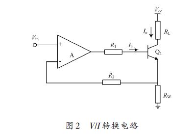
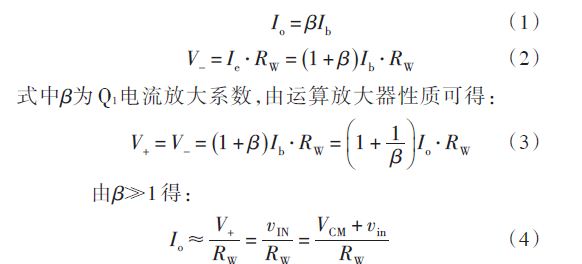
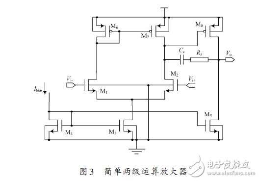
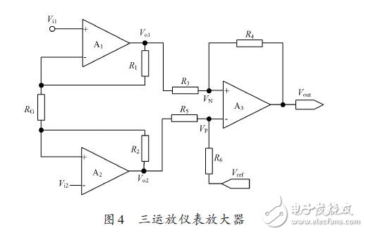
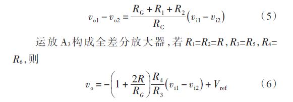
Abstract: In order to solve the problems of linearity and frequency characteristics of traditional optoelectronic isolation, capacitive isolation and transformer isolation, this paper proposes a design scheme of spin valve giant magnetoresistance (GMR) isolation amplifier, and the isolator designed by this scheme. The front-end circuit can convert the input voltage of 0~5 V into 1.4~10 mA current. The back-end receiver circuit has a common-mode rejection ratio of 73 dB when the gain is 1, the gain can be adjusted from 1 to 200, and the working bandwidth is greater than 100. kHz, and use Tanner software to edit, simulate and verify the circuit. The isolator has the characteristics of high sensitivity, good linearity and simple structure, and can be integrated with semiconductor circuits such as silicon. 0 Preface In industrial control, high voltage measurement and medical equipment applications, for safety reasons, it is necessary to introduce electrical isolation in the signal transmission process to reduce the mutual influence of electrical characteristics and interference noise between the ground lines of each equipment. the goal of. Isolators can be divided into analog signal isolators and digital signal isolators depending on the type of signal that needs to be transmitted. Among them, the digital signal isolator has the characteristics of strong anti-interference ability, simple structure and low power consumption, and is used as isolation of binary signals or logic level signals. Analog signal isolators are used to isolate analog signals that change continuously over time. In general, the output of the sensor is almost always a weak analog signal, so the analog signal is amplified before it is isolated. The isolation amplifier is a low noise amplification circuit with a high common mode rejection ratio, which is suitable for isolation between the input analog signal and the data acquisition system. Designing an appropriate amplifier circuit on the periphery of the isolator constitutes an isolation amplifier. Common isolation amplifiers are transformer isolation, capacitive isolation, and opto-isolation. Among them, transformer isolation amplifiers are like AD202 of American Analog Devices, and capacitor isolation amplifiers such as ISO122 of BURR BROWN. They all need external modulation and demodulation circuit modules to make their structure complicated, and optical isolation amplifiers have poor linearity and transmission rate. Lower. In 1998, NVE first introduced a monolithic GMR isolator using a coil to generate a magnetic field for isolation coupling, but only for digital signal isolation. The development of domestic GMR technology is still in its infancy, and the research on isolator based on GMR technology is not yet mature. Here, this paper designs a spin valve GMR isolation amplifier, which is suitable for weak analog signal isolation, featuring high sensitivity, good linearity and simple structure. 1 Basic principle of giant magnetoresistive isolation amplifier The giant magnetoresistive isolator is an isolator based on the giant magnetoresistance (GMR) effect. The so-called giant magnetoresistance effect means that the resistivity of the magnetic material changes greatly when it has an external magnetic field than when there is no external magnetic field. The phenomenon. As shown in Figure 1, the input voltage signal passes through the front-end V/I amplification and conversion circuit of the isolator. The output current flows through the coil to generate a magnetic field proportional to the magnitude of the current. The magnetic field is induced and received by the GMR sensor, and the bridge outputs the output and the magnetic field strength. A linear voltage signal is finally amplified and noise suppressed by the receiving circuit for subsequent circuit processing. The signal remains completely linear throughout the isolation and transmission process. In the GMR isolator structure of Figure 1, the Wheatstone bridge at the bottom uses a spin valve GMR sensor with a large GMR effect, a low saturation field, high sensitivity, and good linearity. The isolation barrier is a tens of micron thick polymer or silicon nitride high-insulation dielectric film with a withstand voltage of 3 000~6 000 V; a spiral rectangular planar coil above the isolation barrier with two opposite current directions Corresponding to the giant magnetoresistance at the opposite diagonal positions of the lower bridge, the magnetic field generated by the coil passes through the isolation grid, changing the resistance state of the resistance at the two diagonal positions, so that the two resistances at one diagonal position are simultaneously high. The resistance state (low resistance state), while the two resistances on the other diagonal position are simultaneously low resistance state (high resistance state). According to the design dimensions of the previous experience coil, the coil efficiency (ie, the ratio of the magnetic field strength generated on the GMR bridge through the isolation barrier to the current flowing through the input coil) is 1.7 Oe/mA. When the current flowing through the coil is -10~ At 10 mA, the linear error of the bridge output voltage is less than 0.05% and the sensitivity is 1.27 mV/V·mA. 2 circuit design and analysis The overall structure of the spin valve GMR isolation amplifier in Figure 1 includes an input stage, an isolation stage, and an output stage. This paper mainly designs the input stage V/I conversion circuit and the output stage back-end receiving circuit, and performs various parameters simulation and verification for each circuit. 2.1 V/I conversion amplifier circuit Because most of the sensor output is weak analog voltage signal, it needs to be amplified and V/I converted before inputting the isolator coil. The conversion circuit is shown in Figure 2. It converts the input voltage signal into a current signal that satisfies a certain relationship. The output current can be kept stable (independent of the load) within a certain load variation range, that is, it has a constant current source characteristic. In order to reduce the power consumption and ensure good linearity of the output, this circuit converts the input voltage signal with the amplitude of 0~5 V into a current signal of 0~10 mA. Let the amplifier A's non-inverting terminal voltage be V+, the inverting terminal voltage be V-, the base current of transistor Q1 be Ib, and the current flowing through the load RL be Io, according to the three-terminal current relationship of transistor Q1: Where VCM is the input bias voltage. It can be seen from equation (4) that the output current is only related to the input voltage and the resistance RW, and is independent of the load RL. Therefore, when signals of different frequencies are input, the output current does not change due to the change of the coil impedance. While ensuring the linearity of signal transmission, it also provides conditions for the design of the back-end receiving circuit to restore the original signal. The precondition for satisfying equation (3) is that A must be an ideal operational amplifier, which requires an infinite open-loop gain, high input impedance, low output resistance, and high common-mode rejection ratio. The operational amplifier uses a simple two-stage operation. Amplification circuit, as shown in Figure 3. A simple two-stage op amp has a common-mode range and large output swing and high gain, but with poor frequency characteristics, small gain bandwidth, and slow speed. Given a certain bias current, the current between the two stages is distributed according to the optimal ratio within the power consumption requirements. The size of each tube is designed reasonably, and the gain, unity gain bandwidth and phase margin of the design are obtained. . 2.2 Receive amplifier circuit Since the operational amplifier of the V/I conversion circuit has a negative feedback effect, the input resistances of the non-inverting terminal and the inverting terminal are not equal or mismatched, resulting in poor common-mode rejection of the circuit. In order to effectively suppress the common mode signal output from the front-end circuit and achieve amplification of the isolator output signal, the instrumentation amplifier is the best choice. It is an optimized precision differential voltage amplifying circuit commonly used in data acquisition systems under harsh environmental conditions. Its main features are: high common mode rejection ratio, low linearity error, high input impedance, low noise and good stability. Unlike conventional op amps, the op amp's closed-loop gain is determined by the external resistor connected between its inverting input and output, while the instrumentation amplifier is determined by an internal feedback resistor that is isolated from the input. In this paper, an instrumentation amplifier with adjustable magnification is designed, as shown in Figure 4. To improve matching, the three op amps in Figure 4 are designed with op amp A in the front-end V/I conversion circuit, where A1 and A2 are non-inverting inputs with high input impedance and perfect match, by op amp Features the output voltage difference of the two op amps: From equation (6), as long as the values ​​of R, R3 and R4 are determined, the voltage gain can be changed by adjusting the resistance of RG. However, R3 and R5 and R4 and R6 should be strictly equal and matched as much as possible, otherwise it will affect the common mode rejection ratio and reduce the anti-interference ability of the instrumentation amplifier. The KSPOWER PUM PUS series is one low profile ultra-thin compact plastic casing, constant voltage mode, wifi bluetooth smart control led driver. Provideing universal AC input 100-240V 50/60Hz and dc output 12 volt 24 volt constant voltage single output wattage 20W 40W 60W 90W with 5 years warranty for home / cabinet / bathroom mirror / stage / strip / puck lighting. The wardrobe led driver is UL CE CCC SAA RoHS FCC Listed and SELV style enclosures. The smart control system led driver support multiple interface and easy for installtion, provides protections for short circuit, over load, over voltage and over temperature. The puck lighting transformers supports each interligent control box (IR/Touch/Door Actived/Hand Move sensor, Wifi, Bluetooth, Tuya App, Smart audio system) works separately and can be used simultaneously in parallel, featuring built-in PFC function more than 0.95 and outstanding led power performance. OEM ODM customization and samples is available. Suitable for dry, damp and wet(optional) locations. smart 12v power supply,smart home adapter (laundry),smart power supply,smart home adapter refrigerator,bathroom mirror led transformer Shenzhenshi Zhenhuan Electronic Co., Ltd , https://www.szzhpower.com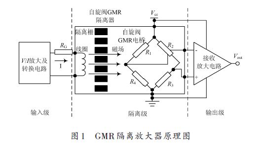
April 17, 2024