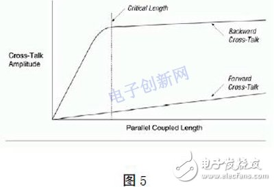
As field-programmable gate arrays (FPGAs) have evolved into true programmable system-on-chips, the task of designing printed circuit boards (PCBs) with these chips has become more complex. To fully implement the functionality of the FPGA, the PCB board needs to be carefully designed. When designing with high-speed FPGAs, it is important to consider several design issues before and during board development. Since the fast switching of I/O signals can cause noise, signal reflection, crosstalk, and EMI problems, you must pay attention to the design: (I) Power Filtering and Distribution The clean, platform-distributed power supply Vcc on all boards and devices reduces system noise. To filter out low frequency (<1kHz) noise generated by the power supply, it is recommended to place a 100uF electrolytic capacitor near the power supply inlet; if using a voltage regulator, place the capacitor directly at Vcc that will ultimately power the device. The capacitor does not filter out the low frequency noise generated by the power supply, but it also provides additional current for many output switchings to occur simultaneously. Another way to filter out power supply noise is to string a ferrite bead and place a 10uf~100uF bypass capacitor on the near magnetic bead. A reasonable terminal, layout, and filtering design does not require magnetic beads, and can be replaced with a 0 ohm resistor. To filter out high frequency noise in the device, it is recommended to place the decoupling capacitor near Vcc and GND. Power distribution also affects system noise. The bus-distributed power and power planes (independent power planes) spread the power to the PCB. Usually the power supply of the two-layer board is distributed by the bus. The density of the PCB limits the width of the trace. The power bus has DC impedance. The last component on the bus receives Vcc, which may be reduced by up to 0.5V. Therefore, it is recommended to use a separate power plane to propagate the power supply, which can effectively reduce the DC impedance. Regarding analog and digital power supplies, if a separate layer is not available, the power plane should be cut. Figure 2 shows an example of PLL power supply isolation. Reduce system noise caused by power distribution: (2) The degree of noise generation, signal reflection, crosstalk, and ground bounce caused by the rapid switching of transmission lines and signal traces depends on the structural characteristics of the PCB raw materials. The dielectric constant of the PCB, Er, The wiring of the microwave transmission line and the ribbon transmission line are as follows: (3) Clock signal routing The following clock routing techniques are recommended: (4) Differential signal routing The following differential signal routing techniques are recommended: (V) Impedance matching and terminal design In order to eliminate signal reflection, the source impedance Zs must be equal to the trace impedance Zo and must also be equal to the load impedance ZL. The load impedance is usually higher than the trace impedance and the trace impedance is higher than the source impedance. To eliminate signal reflections, string in or incorporate some resistors to match ZL or Zs to match Zo. There are many parallel ways. The following describes the common serial matching methods. The serial matching resistor is primarily intended to attenuate secondary reflections. The experience value is recommended to be 33 ohms. For example, we often string a 33 ohm resistor on the trace of the clock signal. (6) Crosstalk Crosstalk refers to the harmful coupling between the parallel lines. Two types of crosstalk: forward (capacitive) and backward (inductive). Forward crosstalk is mainly caused by the mutual capacitance between two long parallel signals, one of which affects the other. Backward crosstalk often occurs in the magnetic region where one signal affects the other. The figure below shows the relationship between the length of the parallel line and the degree of crosstalk.
Qiuck deatail:
Application:
Movie theaters, clubs, stages.
Video processor;controller;video controller Guangzhou Chengwen Photoelectric Technology co.,ltd , https://www.cwledpanel.com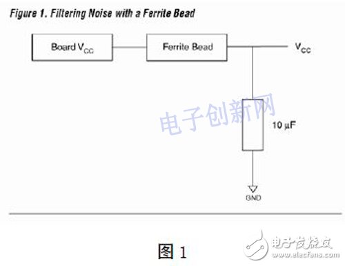
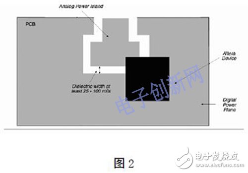
1. Use a separate analog power supply for flat power distribution;
2. PLL power supply avoids traces and multiple signal layers;
3. Simulate a ground level near the PLL power supply surface;
4. Only place analog and digital components on their corresponding ground planes;
5. Use a magnetic bead to isolate the PLL for power and digital power.
Determines the transmission rate of the signal on the board. The following formula is the relationship between the dielectric constant and the signal propagation rate (C = speed of light = 3 & TImes; (10 to the power of 8) m / s):
Vp= C/(Er root number)
Calculate the propagation delay of the signal on the PCB Tpd = l / Vp.
Whether a signal trace is a sample set bus or a distribution line depends on whether the signal switching time (Tr) is greater than 4 Tpd.
Set bus: Tr > 4 &TImes; Tpd
Distribution wiring: Tr < 4 &TImes; Tpd 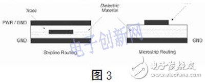
1. Avoid excessive revolving, the clock trace should be as straight as possible;
2. Try to get the clock signal to go only one signal layer;
3. Avoid over-punching in the transmission of clock signals, because the vias will cause impedance changes and reflections;
4. Take the clock signal line in the form of a microwave transmission line (the top layer is more suitable);
5. Close to the outer cloth floor to minimize noise interference, if you use the inner layer to walk the clock signal, use the ground plane to clamp a reduction delay;
6. A suitable termination clock signal line.
1. Ensure D > 2S in the figure to minimize crosstalk;
2. After the signal leaves the device, as close as possible to the two differential signal pairs, minimizing signal reflection;
3. Maintain a constant distance during the entire routing of the two differential signal pairs;
4. Keep the lengths of the two differential signal pairs consistent, minimizing skew and phase differences;
5. Avoid using vias and minimize matching impedance and inductance. 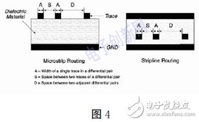
Other Hardware Features
* Business Organizations:
Supermarket, large-scale shopping malls, star-rated hotels, travel agencies
* Financial Organizations:
Banks, insurance companies, post offices, hospital, schools
* Public Places:
Subway, airports, stations, parks, exhibition halls, stadiums, museums, commercial buildings, meeting rooms
* Entertainments:
January 06, 2023