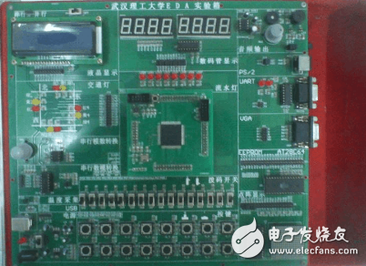
In the traditional hardware circuit design, the main design file is the circuit schematic diagram, and the HDL design system hardware circuit mainly uses HDL to write the source program. (1) VHDL supports top-down and library-based design methods, and supports the design of synchronous circuits, asynchronous circuits, field programmable gate arrays (FPGAs), and other random circuits. (2) The behavior description ability and program structure of the VHDL statement determine that it has the function of supporting the decomposition of large-scale design and the reuse of existing design. It supports the mathematical model of the system until the description of the gate-level circuit, and the high-level behavior description It can be mixed with low-level gate-level circuit descriptions and structure descriptions. (3) The hardware description of VHDL has nothing to do with the specific process technology and hardware structure. When the description at the gate level or above is verified by simulation, the corresponding tools are used to map the design into different processes, so the circuit design and process The changes are independent of each other. Changes to each other do not adversely affect, and the VHDL hardware description language implements a wide range of target devices, using a wide range of CPLDs, FPGAs, and various gate array devices. (4) VHDL has the functions of generic description statement and subroutine call. For the completed design source program, the scale and structure of the design can be changed by modifying the generic parameter table and function. VHDL has a wealth of simulation statements and library functions, making it possible to simulate and inspect the gate-level functions, enabling designers to make decisions about the structural and functional feasibility of the entire engineering design. (5) VHDL as an IEEE industry standard makes VHDL design results easy to reuse and communicate. This further promotes the promotion and improvement of the VHDL language. In addition, due to its rigorous grammar, it brings great convenience to reading and use. The VHDL program of this design mainly has three parts: frequency division, digital tube scanning process, display control process. The schematic of the scheme is as follows. Complete program: Library IEEE; Use IEEE.STD_LOGIC_1164.ALL; Use IEEE.STD_LOGIC_ARITH.ALL; Use IEEE.STD_LOGIC_UNSIGNED.ALL; ENTITY key IS PORT(clk : IN STD_LOGIC; Key : in std_logic_vector(7 downto 0); l : out STD_LOGIC_VECTOR(2 downto 0); Data_o : out STD_LOGIC_VECTOR(7 downto 0); Bell : out STD_LOGIC:='0' ); END key; ARCHITECTURE an OF key IS Signal clk_1k : std_logic; Signal p : integer range 0 to 7; Begin Process(clk) Variable cnt1 : integer range 0 to 200; Variable cnt2 : integer range 0 to 125; Begin If clk'event and clk='1' then If cnt1=200 then Cnt1:=0; If cnt2=125 then Cnt2:=0; Clk_1k"=not clk_1k; Else Cnt2:=cnt2+1; Optical Rotary Sensor,Custom Encoder,Optical Encoder 6Mm Shaft,Handwheel Pulse Generator Jilin Lander Intelligent Technology Co., Ltd , https://www.jilinlandermotor.com

May 21, 2023