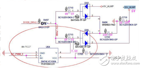
The figure shows a crystal diode-capacitor ten times boost circuit. The circuit can be used as a DC voltage circuit such as an ozone generator or a combustion aid. Crystal Diode-Capacitor Tenfold Boost Circuit When the circuit is not powered, the level is 0V. When power is on, the upper right corner +5V_ALWP charges C710, C722, C715, C719 through the 1 pin of D32. At this time, the potentials at both ends of the capacitor are as shown in the figure above. At this time, the actual level of the +15V_ALWP output port is 5V. When the Y pin of U64 starts to output a square wave with amplitude of 5V, when Y is at 5V for the first time: 1. Since the voltage across the capacitor cannot be abrupt, the voltage across C715 is 5V on the left and 10V on the right. Then the current is charged to the C719 capacitor through the 2 pin of D35. After charging, the voltage of C719 rises to 10V. 2. At the same time, 5V of Y output also charges C710. The voltage across C710 is 5V on the left and 10V on the right. Then the current is charged to C722 through the 2 pin of D32. After the charge is completed, the voltage of C722 rises to 10V. At this time, the actual level of the +15V_ALWP output port is 10V. When the Y pin of U64 starts to output a square wave with amplitude of 5V, when Y is at 0V for the first time: 1. Since the potential across the capacitor cannot be abrupt, the voltage across C715 is 0V on the left and 5V on the right. When the voltage of C715 is 5V, C722 will charge C715 because C722 voltage 10V is greater than 5V of C715. After charging, C715=C722=7.5V. At this time, the voltage of C715 is still lower than the voltage of C719. However, since the D32 diode is reversed, the C719 will not charge the C715. The voltage of C719 is kept at 10V. 2. At the same time, the voltage of C710 is 0V on the left, 5V on the right, and the voltage on the left end of C722 is 7.5V. Due to the reverse cutoff of the 2 pin of D32, C722 will still not charge C710, and C722 will remain at 7.5V. When Y is at 5V for the second time, C722 is charged to 10V through the 2 pins of C710 and D32. When Y is again low, C722 (10V) charges C715 (7.5V). The voltage of C715 becomes 8.75V. After several processes, the voltage difference across C715 rises to 10V. When Y is again 5V, the potential at the right end of C715 becomes 15V. Of course, throughout the process, the C715 is charging the C719 through the 2 pin of the D35. Finally, the level of the +15V_ALWP output port becomes 15V. Motor Start Switch,Single Phase Motor Starter Switches,Single Phase Centrifugal-Switches,Electric Machine Centrifugal Switch Gear Ningbo Zhenhai Rongda Electrical Appliance Co., Ltd. , https://www.centrifugalswitch.com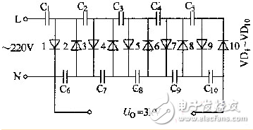
Capacitor diode boost circuit diagram (1)
February 28, 2023