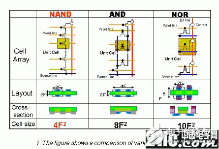
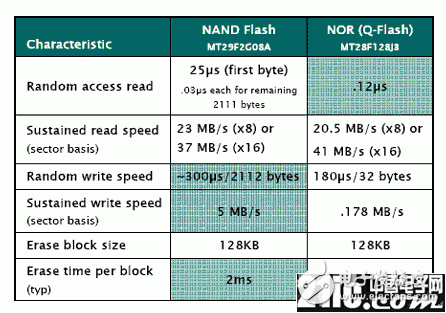
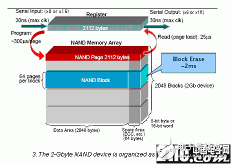
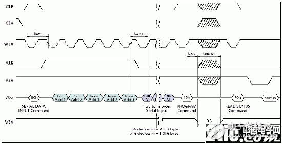
For many consumer audio and video products, NAND flash memory is a better storage solution than hard disk drives, which is evident in low-capacity applications that do not exceed 4 GB. As people continue to pursue products with lower power consumption, lighter weight, and better performance, NAND is proven to be extremely attractive. The NAND flash memory array is divided into a series of 128 kB blocks, which are the smallest erasable entities in the NAND device. Erase a block is to set all bits to "1" (with all bytes set to FFh). It is necessary to change the erased bit from "1" to "0" by programming. The smallest programming entity is the byte. Some NOR flashes can perform both read and write operations (see Figure 1 below). Although NAND cannot perform read and write operations at the same time, it can implement this at the system level using a method called "shadowing." This method has been used on personal computers for many years, that is, the BIOS is loaded from a lower ROM to a higher-speed RAM. NAND is more efficient because there are no metal contacts in the NAND string. The reason that the size of the NAND flash cell is smaller than NOR (4F2: 10F2) is that each cell of the NOR needs a separate metal contact. Similar to hard disk drives, NAND is based on sectors (pages) and is suitable for storing continuous data such as pictures, audio or PC data. Although random access can be implemented at the system level by mapping data to RAM, doing so requires additional RAM storage space. In addition, like hard disks, NAND devices have bad sectors and require error correction codes (ECC) to maintain data integrity. The smaller the memory cell area, the smaller the die area. In this case, NAND can provide a larger flash memory product for today's low-cost consumer market. NAND flash memory is used for almost all erasable memory cards. The NAND multiplexing interface provides a similar pinout for all the latest devices and densities. This pinout allows design engineers to migrate from smaller densities to larger designs without changing the board's hardware design. The advantage of NAND flash is that write (program) and erase operations are faster, and the advantage of NOR is the ability to have random access and perform write (program) operations on the byte (see Figure 2 below). NOR's random access capability supports Direct Code Execution (XiP), a feature that is often required for embedded applications. The disadvantage of NAND is that the random access rate is slow, and the disadvantage of NOR is that it suffers from slow read and erase performance. NAND is more suitable for storing files. Today, more and more processors have direct NAND interfaces and can directly import data from NAND (without NOR). The real benefits of NAND are fast programming and short erase times. NAND supports sustained write operations at speeds exceeding 5 Mbps. Its block erase time is as short as 2ms, while NOR is 750ms. Obviously, NAND has absolute advantages in some aspects. However, it is not very suitable for direct random access. For 16-bit devices, NOR flash requires approximately 41 I/O pins; in contrast, NAND devices require only 24 pins. NAND devices can reuse instruction, address, and data buses, saving pin count. One of the benefits of multiplexing interfaces is that they can use the same hardware design and board to support larger NAND devices. Since the common TSOP-1 package has been used for many years, this feature allows customers to migrate higher density NAND devices to the same board. Another benefit of NAND devices is obviously their package options: NAND offers a thick film 2Gb die or can support up to four stacked dies, allowing an 8Gb device to be stacked in the same TSOP-1 package. This allows a package and interface to support higher densities in the future. Figure 1 Comparison of different flash memory units Figure 2 NOR flash memory random access time is 0.12ms, and the first byte of NAND flash memory random access speed is much slower Taking a 2Gb NAND device as an example, it consists of 2048 blocks, each with 6? Pages (see Figure 3). Figure 3 2GB NAND Flash Contains 2,048 Blocks Each page contains a 2048-byte data area and 6? The free area of ​​bytes contains a total of 2,112 bytes. The free zone is typically used for ECC, wear leveling, and other software overhead features, although it is physically indistinguishable from other pages. NAND devices have 8 or 16-bit interfaces. Main data is connected to the NAND memory through an 8- or 16-bit wide bidirectional data bus. In 16-bit mode, the instruction and address use only the lower 8 bits, while the upper 8 bits are used only during the data transfer period. The time required to erase a block is about 2ms. Once the data is loaded into the register, programming a page takes approximately 300μs. It takes about 25μs to read a page, which involves accessing the storage array page and loading the page into 16-bit, 8-bit, 6-bit registers. In addition to the I/O bus, the NAND interface consists of six main control signals: 1. Chip Enable (CE#): If no CE signal is detected, the NAND device will remain in standby mode and will not respond to any control signal. 2. Write Enable (WE#): WE# is responsible for writing data, addresses, or instructions into the NAND. 3. Read Enable (RE#): RE# allows the output data buffer. 4. Command Latch Enable (CLE): When CLE is high, the instruction is latched into the NAND instruction register on the rising edge of the WE# signal. 5. Address Latch Enable (ALE): When ALE is high, the address is latched into the NAND address register on the rising edge of the WE# signal. 6. Ready/Busy (R/B#): If the NAND device is busy, the R/B# signal will go low. This signal is open-drain and requires pull-up resistors. Each time the data is clocked in/out of the NAND register, it is either a 16-bit or 8-bit interface. When programming, the data to be programmed enters the data register at the rising edge of the WE# signal. Random access or movement of data within registers requires dedicated instructions to facilitate random access. The data register outputs data in a manner similar to that using the RE# signal and is responsible for outputting existing data and adding it to the next address. The WE# and RE# clocks run extremely fast, reaching the 30ns level. When RE# or CE# is not low, the output buffer will be tri-stated. This combination of CE# and RE# enables the output buffer, allowing the NAND flash to share the data bus with other types of memory such as NOR, SRAM, or DRAM. This feature is sometimes referred to as "chip enable don't care." The original intention of this kind of scheme is to adapt to the older NAND device, they require CE# to be low in the whole cycle.
We produce Lighting for commerical ,industrial ,and household . Specially for desk lamp LED which 360 degree bent freely .It can brighten you in any angle as
you want. Road light and functional light also.
Home Outdoor Lighting LED Stadium Light LED Floodlight LED Tri-proof Light LED Street Light LED Garden Light LED Canopy Light Indoor Lighting LED Panel Light LED Batten Light GL Series LED Batten Light GLK Series LED Batten Light
Home Lighting & Furnishings - Quality, Style and Selection. Lamps Plus offers a complete selection of indoor and outdoor lighting fixtures. From stylish ceiling light fixtures, chandeliers and trend-setting ceiling fans to thousands of designer lamps and lamp shades that are in-stock and ready to ship.
Home Light,Led Desk Lamp,Rgb Night Lamp,Bathroom Lights Jiangmen soundrace electronics and technology co.,ltd. , https://www.soundracegroup.com


April 23, 2023