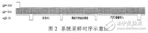
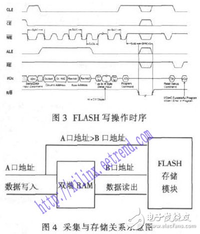
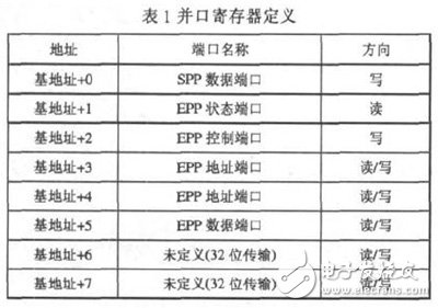
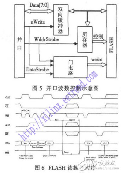
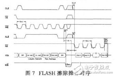
Data acquisition and storage is an important part of the signal processing process, and has been widely used in radar, sonar, transient signal testing, wireless flaw detection and other fields. The sampling rate and sampling accuracy are also different under different conditions, and the implementation methods of the system are also different. Typically, acquisition and data computer reads can occur simultaneously if the acquisition rate is low. However, in the case of high-speed acquisition or acquisition source movement, such as an aerial flying body or an underwater moving body, it is necessary to have a storage function while the system has an acquisition function, and the stored data can be read afterwards, and the black box belongs to such an acquisition. Memory. According to the current development trend, systems with small size, low power consumption and large storage capacity are receiving more and more attention. Based on the actual situation, we have developed a recyclable small-volume, low-power, large-capacity memory that can be used underwater and can be used underwater. This paper introduces a design and implementation method of multi-channel and large-capacity acquisition memory based on FPGA and FLASH. When the ship or submarine is moving in the water, it is necessary to record the transient parameters of the change parameter signal during the movement, and the record memory is to be installed on the moving hull or the hull. The acquisition storage time is not long, but it must meet the small size, low power consumption and rewritable function. This system requires 32 channels of analog signals to be simultaneously collected and stored. The sampling rate is 10KHZ per channel, and the total sampling rate is 320K. Afterwards, the stored data can be read and analyzed. According to this requirement, we designed and implemented a multi-channel acquisition memory, which uses FPGA and FLASH memory. Meet the requirements of small size and low power consumption. It works with a dry battery. The entire system uses FPGA as the core controller to organize the work, which controls the reading, writing, erasing and other operations of the entire system. The main problem solved by the system is the acquisition, storage and data read afterwards. Due to the simultaneous acquisition of multiple signals, we have adopted an FPGA to perform equal time advancement of the analog switches to achieve channel conversion. When converting to a channel, the FPGA also starts A/D for analog-to-digital conversion. For the purpose of high precision acquisition, a 12-bit AD converter can be used. In order to achieve reasonable timing of channel conversion, start A/D and data FIFO storage, we use the entire clock, the implementation process is shown in the figure below. For data storage, we use FLASH Memory as the memory, which has the characteristics of small size, low power consumption and data loss. The FLASH write operation has its fixed operation mode, as shown in Figure 3. Since FLASH is stored by page, when a page is written, the control word and address of the next page are rewritten, so that the collected data can be written into FLASH in time and accurately, without being on the page and page. The data is lost in the alternate time, so it is impossible to store the collected data directly into the FLASH. We use the RAM provided in the FPGA to form the dual port RAM as the buffer in the data storage process. The collected data is first written to the dual port. RAM, then import FLASH. The process is to retrieve data from port A to the dual port RAM. The data in the dual port RAM is read from the B port and then written to the FLASH. During the operation, it is necessary to ensure that the port B address of the dual port RAM advances less than the address of the port A. Because 12 bits of AD are used in the acquisition process, and the FLASH memory is 8-bit memory, the data collected each time is stored in 2 times. The way we take it is to store the high 8 bits once and the lower 4 bits. The supplemental flag code is stored once. There are many ways to read data. Currently, there are serial port, parallel port, USB port or PCI bus mode. We use the parallel port reading method here. Because of the large amount of data storage, we have adopted the method of active reading by the parallel port, which eliminates the problem of slow reading speed of the parallel port. With the EPP mode, the data speed can reach 500K-2Mb/s. The FPGA's job at this point is to isolate the readings and acquisition control lines from the data lines. At this time, the parallel port can directly operate the control line and data line of the FLASH. The FLASH reading operation also has its fixed operation. The erasure of FLASH data is erased in blocks, so it is characterized by a fast erase speed, which is usually completed in a few seconds. When the acquisition is completed, the data will remain in the FLASH for a long time and will not be lost. To acquire the storage again, the FLASH erase must be performed first. Screen Protector Cutting Machine Tpu Hydrogel Cutting Plotter,Inteligent Screen Protector Cutter,Mobile Phone Cut Plotter,Screen Protector Cutter Shenzhen TUOLI Electronic Technology Co., Ltd. , https://www.szhydrogelprotector.com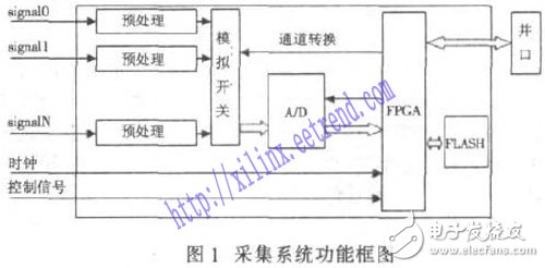
January 19, 2023