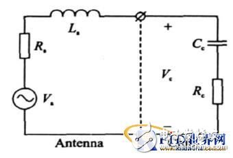
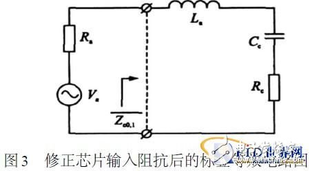
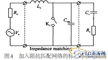
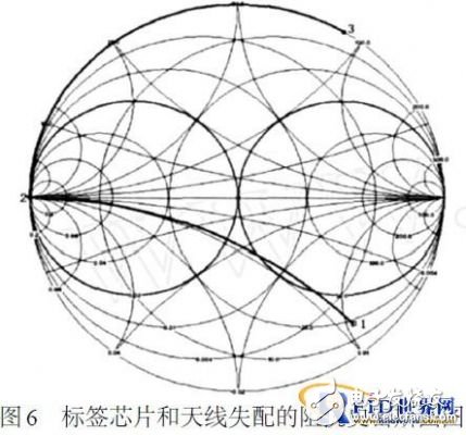
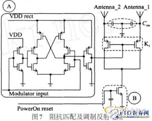
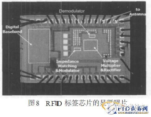
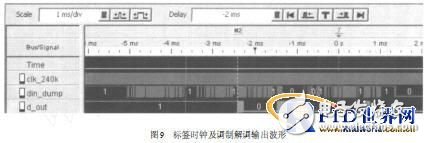
RFID (RadiofrequencyidenTIficaTIon) is a rapidly developing automatic identification technology that has been developed in recent years. It uses radio frequency for non-contact two-way communication to achieve the purpose of identification and exchange data. As the basis for high-tech and information standardization of fast, real-time and accurate information collection and processing, RFID has broad application prospects in various industries such as production, retail, logistics and transportation. RFID technology has been recognized by the world as one of the ten most important technologies of this century. An RFID tag contains an antenna and a chip, both of which have a complex impedance. For passive tags, because the power consumption required for tag operation is all derived from the RF energy emitted by the reader, whether the antenna and the chip can achieve good matching and power transmission directly affects the realization of the system function. The key performance of the label is largely determined. At present, the existing impedance matching methods are mostly complicated, and the accuracy of label recognition is low when used for an RFID chip, and the effect is not satisfactory. In this paper, a design method of low-cost impedance matching network for passive RFID tag chip is proposed. The matching network is integrated in the tag chip and has a simple structure. It is realized between the tag antenna and the chip and between the tag and the reader. The maximum power transmission improves the performance of the chip and improves the recognition rate of the tag reflection signal by the reader. 1.1.1 RFID principle and label composition Common RFID systems consist primarily of readers and tags. The reader sends a radio frequency continuous wave (ConWInuous2wave, CW for short) to the tag, activates the tag chip and modulates the command and data into the radio frequency electromagnetic wave. The tag in the electromagnetic field of the reader increases the smaller input voltage to the voltage required for the normal operation of the tag chip through the voltage doubler rectifier circuit, and converts the alternating current into direct current; The output voltage is unstable and needs to be added to the voltage stabilizing circuit; the tag demodulation module demodulates the command and data from the received radio frequency continuous wave and sends it to the digital baseband module; the digital baseband module completes according to the received command according to the protocol. Data storage, transmission or other operations [4]; when returning data, the tag changes the reflection coefficient of the antenna by changing its impedance, and sends the modulated reflection signal back to the reader. The clock generation circuit provides the clock frequency required for the chip operation, and is calibrated by the clock calibration information sent by the reader to realize clock synchronization; the power-on reset circuit resets the baseband processor on the one hand, and enables the modulation and reflection circuit on the other hand. signal. Figure 1 shows the block diagram of the RFID tag system. The chip contains three parts: RF analog front end, digital baseband and non-volatile memory (NVM). The basic functions of the analog front end include: impedance matching, voltage doubler rectification, modulation, demodulation, voltage regulation, power-on reset, clock generation, and so on. Figure 1 Block diagram of the RFID tag system 1.1.2 Impedance matching analysis Figure 2 shows the tag's Thevenin equivalent circuit, which has been used by many researchers to solve various antenna problems. The open circuit AC voltage induced by the RF signal on the antenna is Va, the chip input voltage is Vc, the antenna input impedance Za=Ra+jXa, and the chip input impedance Zc=Rc+jXc. The real part of the chip input impedance is mainly determined by the voltage doubler rectifier circuit and the load, and the imaginary part is mainly determined by the voltage doubler rectifier circuit, the modulation and demodulation circuit and the ESD. Both Za and Zc vary with operating frequency, and in practical applications, the value of Zc varies with different input powers. In this paper, the design of the impedance matching network is completed with the input power equal to the minimum power required for the normal operation of the chip. In order to achieve maximum power transfer, the input impedance of the chip must be conjugated to the antenna. Figure 2 RFID tag equivalent circuit diagram L-type matching is an impedance matching method used to achieve high-efficiency conversion from RF to DC. The matching effect is achieved by the series inductance and the capacitance resonance in the chip. For RFID tag chips, it is unrealistic to integrate the inductor in a small area. Therefore, the input impedance of the chip is corrected by the following method to achieve the purpose of L-type matching using the inductance La. In the case where two devices with complex impedances are directly connected, the complex power wave reflection coefficient at the interface is defined as s, which can be applied to RFID tags: The input impedances of the chip in the conjugate matching (state 0) and mismatch (state 1) of the antenna impedance are Zc0 and Zc1, respectively. Through the impedance correction, the imaginary part of the antenna impedance is added to the chip, and the corrected antenna impedance is only The real part Ra is retained, as shown in Figure 3. The input voltage of the chip can be calculated by equation (3): Since the energy required for the operation of the passive RFID chip is completely derived from the space electromagnetic field, the input voltage Vc has a sufficiently high value that the voltage-doubler rectifier circuit can be turned on and provides a normal operating voltage, and is also an important parameter determining the performance of the tag. The RCS (radar cross section) of the RFID tag is a function of the input impedance of the chip. The value of the RCS is obtained by the classical radar equation: Where K is the wavelength and G is the tag antenna gain. The different RCS values ​​corresponding to the input impedance state of the two chips allow the reader to distinguish the data transmitted by the tag from the amplitude of the modulated reflected signal. The vector differential RCS further allows the reader to detect the relative phase characteristics of the modulated reflected signal. Label the vector with ΔV: 2.1.1 Principle analysis When the tag is operating in the 923MHz band and the chip is in the minimum input power, the Agilent E5071C network analyzer measures the input impedance of the chip that is not added to the impedance matching network to 22-j106 ohms. According to the input impedance characteristics of the chip, a tag antenna with a large Q value is selected. The input impedance of the antenna is 15+j88 ohms. The design of the impedance matching network is shown in Figure 4, where La = 1512 nH. When switch K1 is open, the chip is in state 0. In the matching path from the input impedance of the tag chip to the conjugate impedance of the antenna shown in FIG. 5, the impedance at point 1 is 22-j106 ohms; after the parallel capacitor Ccm, the resistance at 158 ​​is rounded at point 2, and the impedance is 15- J888; the series inductance La reaches point 3, and its impedance is 158, which is conjugate matched with the corrected antenna impedance Ra. It is calculated that Ccm = 340fF can be obtained. There is no complex power wave reflection at the antenna and chip interface. The conjugate matching between the chip and the antenna allows the antenna to transmit half of the RF energy received from the air to the chip to maximize power transmission. When the switch K1 is closed, the chip is in state 1. Figure 6 shows the path of the change in input impedance of the tag chip. 2.1.2 Performance Comparison In the case where impedance matching is not performed, the value of the chip Qc is 4182; after the impedance matching network is added, Qc is increased to 5187 under the conjugate matching state of the chip and the antenna impedance, and the exchange obtained by the chip is obtained by the formula (3). The voltage Vc is increased by 111 times, which improves the performance of the chip. By comparison, the modulus of the vector differential RCS of the chip is 1015dB, which greatly improves the recognizability of the reflected signal of the tag and improves the accuracy of the tag recognition by the reader. 2.1.3 circuit implementation The impedance matching network consists of two parts, capacitor Ccm and switch K1, as shown in Figure 7. In order to ensure the symmetry of the circuit between the two antenna pins, Ccm adopts two capacitors in parallel, each of which is 170fF; K1 is composed of two PMOS switch tubes, and the PMOS is passed through the level conversion circuit by the baseband signal (Figure 7A) Partially) drive, so the gate of the PMOS can obtain a higher gate voltage, ensuring that the off state is reliably cut off; part B is the power-on protection circuit, ensuring that the power-on reset signal given by the digital baseband is in a stable state. Into the modulation reflection, avoiding the reflection of the chip in the absence of working energy due to the uncertainty of the state before the digital baseband circuit is reset. Both the PMOS switch tube and the NMOS power-on protection tube adopt a mesh gate structure, which increases the width-to-length ratio of the MOS tube, which is beneficial to reducing the resistance and parasitic capacitance of the MOS tube. The designed RFID tag chip is based on charted0135Lm2P4M, low threshold CMOS process flow chip, chip size 1026Lm & TImes; 1796Lm, Figure 8 is a photomicrograph of the chip. In actual use, the chip has only two pins connected to the antenna. The remaining pins shown in the figure are used for testing, and the corresponding analog or digital signals are connected. The output level of the voltage doubler circuit is an important indicator to determine the performance of the RFID chip. When the input AC level is only 300mV, the output DC level of the chip can reach 1147V, which fully meets the level requirements of the normal operation of the chip. . The RFID operating band specified in 1800026C is 860 to 960 MHz, which coincides with the regulation of China [11] in the 920-925 MHz frequency band. Therefore, the designed RFID tag operates in the 923 MHz band. Using Impinj's speedway reader, set the transmit power to 2WERP and the tag antenna gain to 115dBi for testing in free space. The signal waveform is tested using the Agilent 1682A logic analyzer. Figure 9 shows the “clk-240k†as the system operating clock with a frequency of 240 kHz; “din-dump†is the demodulated output signal; “d-out†is the modulated output signal. Tests show that the tag using the impedance matching network has a bit error rate lower than 10-4 during communication with the reader, and the tag is more accurately identified at a time. A low-cost impedance matching network for passive RFID tags conforming to the ISO1800026C standard is proposed. The circuit structure is simple, and the power transmission is maximized between the reader, the tag antenna and the chip. The tag chip using this impedance matching method has been verified by the charted0135LmCMOS process. Theoretical analysis and measured results show that the method effectively improves the performance of the chip, improves the accuracy of the reader recognition of the tag, and the tag meets the system design requirements.
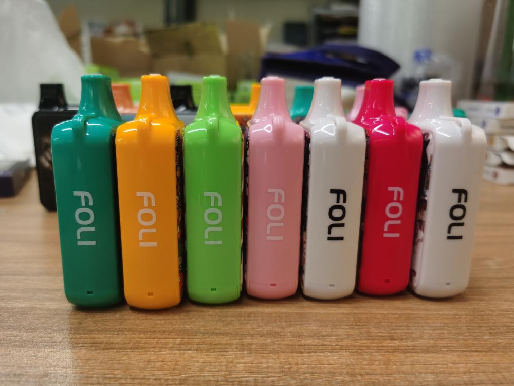
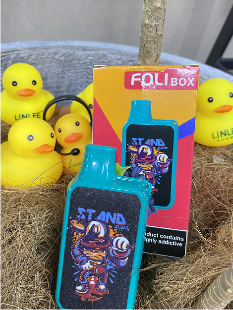
FOLI has many types of disposables vape; FOLI BOX is one of popular Disposable Vape.
5000 Puffs, Mesh Coil, good cigarette oil, good, tasty and the price is reasonable. The minimum order quantity is 30 pieces, in stock, and delivered on the same day. It only takes 7-10 days from China to destination. Please take an order if you are interested.
Foli Vape is a hot vape brand in many countries. Foli Disposable Vape provides an innovative leak-resistant maze coil, ensuring security wherever you are and regardless of your daily activities.Foli Box disposable vape is rich in flavors, with 16 taste choices. The bottom suction resistance adjustment button can adjust the suction resistance according to personal preference.FOLI Box disposable vape is bright and colourful, and is deeply loved by young people.
Foli Disposable Vape,Big Smoke High-Power Vape,E Cigarette Atomizer ,Disposable Vape Mash Coil Tsvape E-cigarette Supplier Wholesale/OEM/ODM , https://www.tsecigarette.com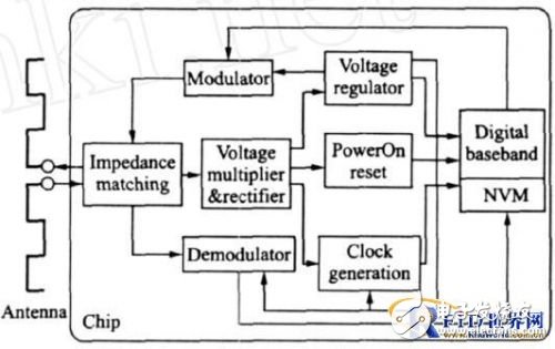





Disposable Vape FOLI BOX 12ml 5000 Puffs Big Smoke rechargeable
600mah A-level battery
12ml eujice & 1.2ohm
16 flavors available Outstanding Flavor
Nicotin 3%
Puffs: 5000 Puffs
Volume:12ml
Battery Capacity:600mAh
Charging Port:Type-C
Suction resistance adjustment button
Flavor List:
MINT
LYCHEE STRAWBERRY
GREEN APPLE
WATERMELON
ORANGE MANGO
STRAWBERRYICECREAM
CRANBERRYGRAPE
GRAPE
BLUEBERRYRASPBERRY
LEMON TEA
BANANA LYCHEE
SKITTLES
GOLDEN FRUIT
BLUEBERRY
WATERMELON LYCHEE
STRAWBERRY
Features
1. No other carcinogenic substance.
2. Harmless to others and the environment. With no danger of second-hand smoking.
3. Smoke in public places, business, restaurants, planes etc. Does not emit any smell.
4. Enable smokers to abstain from smoking non-painfully.
5. Save the smoking cost of nearly 80% each year.
6. No ignition and no fire danger.


February 13, 2023