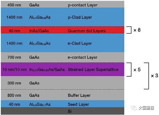
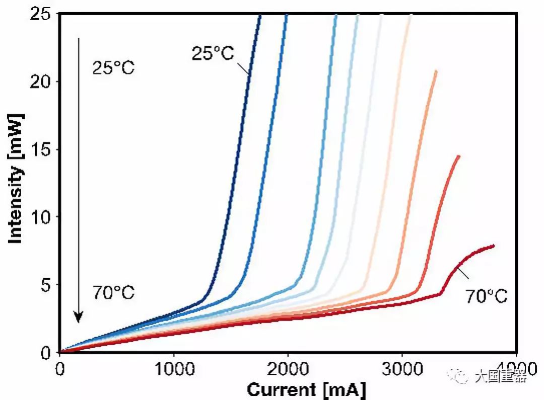
A research team from the University of Tokyo, Japan, claimed that for the first time, a material growth process for electrically pumping 1.3 μm indium arsenide (InAs) in a silicon substrate gallium arsenide (GaAs) quantum dot (QD) laser has been realized. Molecular beam epitaxy (MBE) is used to grow directly on a coaxial (001) silicon substrate. Figure 1 shows the InAs / GaAs QD laser material grown on a coaxial Si (001) substrate. Traditional methods Growth along the 001 axis of silicon usually begins with Metal Organic Chemical Vapor Deposition (MOCVD) technology, which in turn grows molecular beam epitaxial quantum dot layers. Alternative techniques for implementing molecular beam epitaxy techniques include cutting the substrate to prevent crystal defects such as threading dislocations (TDs), reversed-phase boundaries (APBs), and cracks. Unfortunately, off-axis silicon is incompatible with mainstream CMOS electronics. MOCVD cannot effectively filter dislocations or produce highly efficient quantum dots. significance The team believes that the development of 1.3μm lasers will help promote silicon photonics "to solve the next generation of computing low bandwidth density and high power consumption and other metal wiring issues." new method The researchers used the n-type substrate as a molecular beam epitaxy solid source (Figure 1). The chamber was first heated to 950°C for 5 minutes to anneal the substrate, and then a series of three-layered 300 nm GaAs layers were grown, followed by the InGaAs / GaAs strained superlattice, thereby impeding the penetration dislocations from reaching the quantum dot layer. The threading dislocation density in the quantum dot region is about 5×10 7 /cm 2 . The team pointed out that thermal cyclic annealing during the deposition process may result in lower density. For the AlGaAs layer, a growth temperature of 500[deg.] C. and a higher growth rate of 1.1 [mu]m/hour avoids the anti-phase boundary, so that the anti-phase boundary quenches within 400 nm of the GaAs buffer deposit. Experimental results Quantum dots measure approximately 30 nm in the lateral direction and have a density of 5×10 10 /cm 2 . Photoluminescence from this structure has an intensity of 80% from the structure grown on a GaAs substrate. The peak wavelength is 1250 nm and the full width at half maximum is 31 meV. A 1150 nm (+ 86 meV) excitation level is also seen in the spectrum. This material was fabricated as a 80 [mu]m wide wide area Fabry-Perot laser. The contact layer is gold-bismuth-nickel/gold. The backside of the substrate is thinned to 100 μm. The structure was then cut into 2mm long lasers. The mirror is cut without applying a high-reflectance coating. Under the pulse injection, the lowest laser threshold current density is 320A/cm2. The maximum output power of a single face exceeds 30mW. When measured in the 25-70°C range, the laser threshold has a characteristic temperature of 51K. At 25 °C, the slope efficiency is 0.052 W / A. With continuous wave current injection up to 1000mA, the device does not emit laser light. Figure 2 shows the temperature-dependent optical output power and current curve of a pulsed laser The researchers stated that lasers grown on silicon wafers exhibit “degradation in several characteristics such as output and thermal characteristics†compared to devices grown on GaAs substrates. The team hopes to optimize the growth process, especially the seed layer, to improve the performance of the laser. Solutions,Networking Solution,Network Solutions,Beyond Networking Solution Huizhou Fibercan Industrial Co.Ltd , https://www.fibercannetworks.com

April 23, 2023