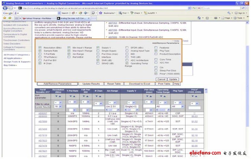
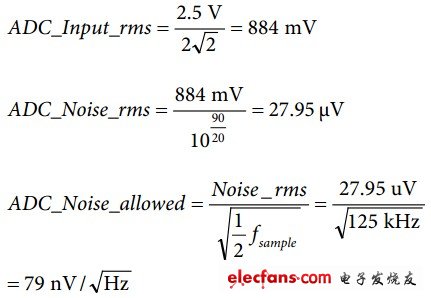
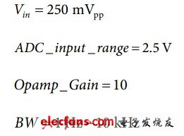
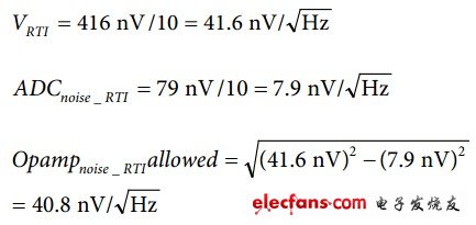
Real-world signals such as vibration, temperature, pressure, and light require precise signal conditioning and signal conversion before further data processing in the digital domain. To overcome the many challenges of today's high-precision applications, a well-designed low-noise analog front end is required to achieve the best signal-to-noise ratio (SNR). Many systems can't afford the most expensive devices, nor can they withstand the higher power consumption of low-noise devices. This paper presents a systematic approach to design a gain block and ADC combination and gives an example of supporting this method. The circuit performs noise calculations and analysis while conditioning low frequency (close to dc) signals. Figure 1 Typical signal conditioning chain When designing an analog front end, follow these seven steps: 1) Describe the electrical output of the front of the sensor or gain block 2) Calculate the needs of the ADC 3) Find the best ADC + reference voltage for signal conversion 4) Find the maximum gain for the op amp and define the search criteria 5) Find the best amplifier and design the gain module 6) Check the solution total noise according to the design target 7) Run the simulation and verify Step 1: Describe the electrical output of the front of the sensor or gain block The signal may be sourced directly from the sensor or it may pass through the EMI and RFI filters before reaching the gain block. In order to design the gain block, the ac and dc characteristics of the signal and the available power supply must be known. Knowing the characteristics of the signal and the noise level, we know what input voltage range and noise level are needed to select the ADC. Suppose there is a sensor that outputs a 10 kHz signal at full scale amplitude of 250 mV pp (88.2 mV rms) and 25 μV pp noise. We further assume that there is a 5V power supply available in the system. With this information, we should be able to calculate the signal-to-noise ratio at the ADC input in step 2. To simplify data processing and avoid confusion, let's assume that the solution is designed to work at room temperature. Step 2: Calculate the ADC requirements What kind of ADC do we need, what is the sampling rate, how many bits, and what are the noise specifications? If we know the input signal amplitude and noise information from the first step, we can calculate the signal-to-noise ratio (SNR) at the input of the gain block. We need to choose an ADC with a better signal to noise ratio. Knowing the SNR will help us calculate the effective number of bits (ENOB) when choosing an ADC. This relational expression is as follows. The ideal ADC data sheet always marks SNR and ENOB. The 86.8 dB SNR and 14.2 ENOB required in this example determine that we should choose a 16-bit analog-to-digital converter. In addition, the Nyquist criterion requires that the sampling rate (fs) be at least twice the maximum input frequency (fin), so a 20-kSPS ADC should be sufficient. Next we need to design the overall solution so that the noise density does not exceed 416 nV/rt-Hz. Step 3: Find the best ADC+ reference for signal conversion With a range of search criteria, we have many ways to find the right ADC. One of the easiest ways to find a 16-bit ADC is to use the search tool on the manufacturer's website. Enter the resolution and sample rate to find many recommended ADCs. Many 16-bit ADCs meet the 14.5-bit ENOB requirement. If you want better noise performance, you can use oversampling to force ENOB up to 16 bits (next enhancement by 4^n oversampling). With oversampling, you can use a lower resolution ADC: a 256 oversampled 12-bit ADC (4^4 oversampling) for 16-bit noise performance. In our case, this means a 12.12 MHz sample rate 12-bit ADC (20 kSPS & TImes; 256), or a 4^2 oversampled 14-bit ADC; if 1.28 MSPS is better. However, the cost of these options is comparable to the AD7685 (16-bit, 250 kSPS ADC). Figure 2 Typical ADC Selection Table From the list we chose the AD7685 (16-bit PulSAR ADC). The converter has a 90-dB SNR and a 250 ksps sampling rate to meet our needs. This ADC is recommended for use with the ADR421/ADR431 precision XFET reference. The 2.5-V input range exceeds the 250-mV pp input characteristics we need. The AD7685 reference input has a dynamic input impedance and therefore needs to be decoupled to minimize parasitic inductance by placing a ceramic decoupling capacitor near the pin and connecting it with a wide low impedance trace. A 22 μF ceramic chip capacitor provides the best performance. Step 4: Find the maximum gain for the op amp and define the search criteria Having the input voltage range of the ADC will help us design the gain block. To maximize dynamic range, we need to choose the highest possible gain for a given input signal and ADC input range. This means that we can design the gain block in this example to have a gain of 10 times. Although the AD7685 is easy to drive, the driver amplifier needs to meet certain requirements. For example, to maintain the SNR and conversion noise performance of the AD7685, the noise generated by the driver amplifier must be as low as possible, but be aware that the gain block can amplify both the signal and the noise. To keep the noise constant before and after the gain block, we need to select the amplifier and associated components with lower noise values. In addition, the driver's THD performance should be comparable to that of the AD7685, and the ADC capacitor array must be built to a full-scale step at 16-bit levels (0.0015%). The noise from the amplifier can be further filtered using an external filter. How much noise does the input of the op amp allow? Keep in mind that the overall solution we designed does not exceed 416 nV/rt-Hz. The gain block we designed should have a lower noise floor with a factor of 10 because our gain is 10. This will ensure that the noise from the amplifier is much lower than the noise floor of the sensor. When calculating the noise margin, we can assume that the noise at the input of the op amp is roughly equal to the total noise of the op amp plus the noise of the ADC.
All In One Gaming PC is the best choice when you are looking higher level desktop type computer for heaver tasks, like engineering or architecture drawings, designing, 3D max, video or music editing, etc. What we do is Custom All In One Gaming PC, you can see Colorful All In One Gaming PC at this store, but the most welcome is white and black. Sometimes, clients may ask which is the Best All In One Gaming PC? 23.8 inch i7 or i5 11th generation All In One Gaming Desktop PC should beat it. Cause this configuration can finish more than 80% task for heavier jobs. Business All In One Computer and All In One Desktop Touch Screen is other two popular series. Multiple screens, cpu, storage optional. Except All In One PC, there are Education Laptop, Gaming Laptop, i7 16gb ram 4gb graphics laptop, Mini PC , all in one, etc.
Any other unique requirements, Just feel free to contact us and share your ideas, thus more matched details sended in 1-2working days. Will try our best to support you.
Of course, any we can do in China, also willing to do it for you.
All In One Gaming PC,Best All In One Gaming Pc,Colorful All In One Gaming Pc,Custom All In One Gaming Pc,All In One Gaming Desktop Pc Henan Shuyi Electronics Co., Ltd. , https://www.shuyipc.com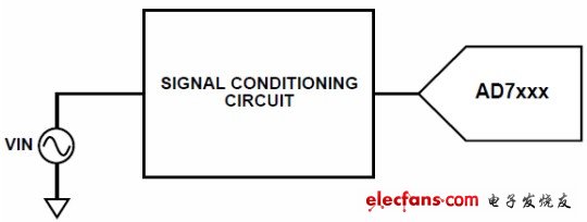

November 05, 2024