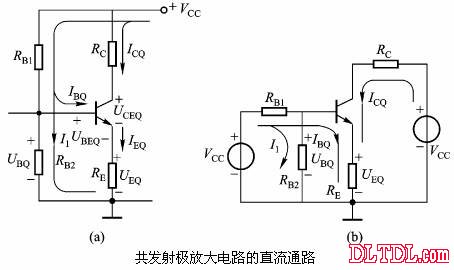
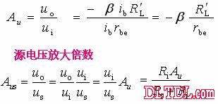
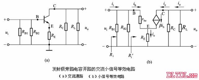
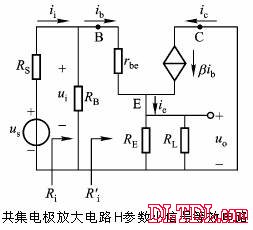
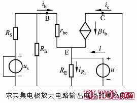
Transistor amplification circuit analysis and calculation First, common emitter amplification circuit (1) The composition of the circuit: the power supply VCC obtains the appropriate bias of the transistor through RB1, RB2, RC, RE, and provides the necessary conditions for the amplification of the triode. RB1 and RB2 are called base bias resistors, and RE is called The emitter resistance, RC is called the collector load resistance, and uses the step-down effect of RC to convert the change of the collector current of the triode into the change of the collector voltage, thereby realizing the voltage amplification of the signal. The capacitor CE in parallel with the RE is called the emitter bypass capacitor, which is used to short-circuit the AC, so that the RE does not affect the voltage amplification factor of the amplifier circuit, so the smaller the capacitive reactance of the signal frequency is, the better. In the low frequency amplifier circuit, the CE usually also uses an electrolytic capacitor. Vcc (DC power supply): The emitter junction is forward biased, and the collector junction is reverse biased; power is supplied to the load and components. C1, C2 (coupling capacitor): DC and AC; RB1, RB2 (base bias resistor): provide suitable base current RC (collector load resistance): Will DIC ? DUC be used to amplify the current? Voltage amplification RE (emitter resistance): stable static operating point "Q" CE (emitter bypass capacitor): short-circuit AC, eliminating the effect of RE on voltage amplification (2) DC analysis: Open all the capacitors in the large circuit, that is, get the DC path. As shown in the figure below, this circuit is also called the voltage-divider-biased operating point to stabilize the direct current path. Circuit operation requirements: I1 3 (5~10) IBQ, UBQ3 (5 ~ 10) UBEQ Find the static working point Q: Method 1. Estimate The main reason for the instability of the working point Q: Vcc fluctuation, triode aging, temperature change stable Q point principle: Method 2. Use the Thevenin Theorem for IBQ (III) Analysis of performance indicators The C1, C2, and CE in the amplifying circuit are short-circuited, and the power supply Vcc is short-circuited to obtain an AC path. Then, the triode is substituted with the H-parameter small-signal circuit model, and the small-signal circuit model of the amplifying circuit is obtained as shown in the following figure. Voltage amplification 2. Input resistance calculation 3. Output resistance Ro = RC When there is no bypass capacitor CE: Voltage amplification Source voltage amplification 2. Input resistance 3. Output resistance Ro = RC Second, the common collector amplifier circuit (emitter output, emitter follower) (1) Circuit composition and static working point The common collector amplifier circuit is shown in Figure (a) below, and Figures (b) and (c) are its DC path and AC path, respectively. Seen from the AC path, the collector of the triode is the AC ground potential, the input signal ui and the output signal uo are common to it, so it is called the common collector amplifier circuit, and because the output signal uo is taken from the emitter, it is also called the shot. Polar output. IBQ = (Vcc - UBEQ) / [RB + (1 + b) RE] ICQ = bIBQ, UCEQ = Vcc - ICQRE (II) Analysis of performance indicators Voltage amplification 2. Input resistance R¢L=RE//RL 3. Output resistance Common collector circuit characteristics common collector circuit use 1.Uo is in phase with Ui and has voltage follow-up effect. 1. High impedance input stage 2. No voltage amplification Au<1 2. Low impedance output stage 3. Input resistance is high; output resistance is low 3. Intermediate isolation level First, common base amplifier circuit The common base amplifier circuit is shown below. It can be seen from the figure that the AC signal is grounded through the base bypass capacitor C2 of the transistor, so the input signal ui is introduced by the emitter and the output signal uo is taken out by the collector, and they are all common at the base, so it is called a common base amplifying circuit. From the perspective of the DC path, it also constitutes a voltage-divided current negative feedback bias. (1) Seeking "Q" (II) Analysis of performance indicators RO=RC (III) Features: The common base amplifier circuit has the characteristics that the output voltage is in phase with the input voltage, the voltage amplification factor is high, the input resistance is small, and the output resistance is large. Since the common base circuit has good high frequency characteristics, it is widely used in high frequency or wideband amplification circuits. China 433/868/915MHz Antenna,High gain 433/868/915MHz Antenna.Factory Price 433/868/915MHz Antenna 433MHz Antenna.868MHz Antenna.915MHz Antenna Yetnorson Antenna Co., Ltd. , https://www.xhlantenna.com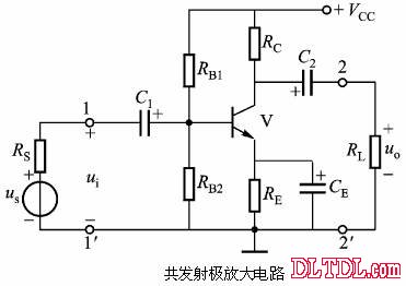





![]()


October 06, 2022