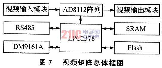
Abstract: Using NXP's ARM7-based microcontroller LPC2378 and ADI's video matrix switching chip AD8112, a video matrix switching device is designed. With the support of μC/OS-II embedded operating system, Ethernet is realized. Video matrix of 64 channels of video input and 8 channels of video output. This article refers to the address: http:// Introduction The video surveillance system has evolved in just over two decades. From the earliest analog surveillance to the hot digital surveillance of previous years, to the current network video surveillance, earth-shaking changes have taken place. Video surveillance systems have been used more and more widely in ports, factories, banks, airports, and transportation. In a large-scale monitoring system, since there are many monitoring points, there are many video images to be monitored, so a large number of cameras are required. The number of monitors and live cameras in the monitoring center is generally 1:5 to 1:10, so the video matrix switching device plays an important role in the entire monitoring system. 1 LPC2378 Features LPC2378 includes 10/10OM Ethernet MAC, USB 2.0 full speed interface, 4 UARTs, 2 CAN channels, 1 SPI interface, 2 synchronous serial ports (SSP), 3 I2C interfaces, 1 I2S interface, MiniBus, 4 general purpose timers, 10-bit A/D converter, RTC, watchdog and 104 general purpose I/O pins. The features of the LPC32378 are as follows: 2 AD8112 Features The AD8112 is a 16-input, 8-output video matrix switching chip from Analog Devices, Inc. All inputs and outputs are cached. The AD8112 has a switch matrix of 128 independent electronic switches that can implement 16 video inputs and 8 video outputs. The matrix switching is 100% non-blocking. By writing the control series word through serial or parallel programming, any one input and any one output connection can be enabled, and each output can be connected with any one of the 16 pseudo input signals. The functional block diagram of the AD8112 is shown in Figure 1. 3 The composition of 128 × 16 video matrix This design uses 4 AD8112 to form a video switching matrix, which realizes video switching of 64 video input and 8 video output. Connect the corresponding pins of each AD8112 in parallel. When one of the AD8112 pins is enabled, the corresponding pins of other chips will be set to the disabled state to ensure that the output does not conflict when the video is switched. At the time of power-up, all output pins are initialized to a disabled state to prevent output conflicts. The connection method is shown in Figure 5. 4 video matrix overall design The overall block diagram of the video matrix is ​​shown in Figure 7. The AD8112 array consists of four AD8112 chips. After switching 64 channels of signals input through the video input module, eight signals are output through the video output module to achieve 64×8 video information switching. Ethernet interface module DM9161A peripheral circuit PHY chip is connected to LPC2378 through RMII interface, which is easy to implement Ethernet communication function. The RS485 communication module controls the camera pan/tilt in serial communication mode. 5 video matrix control word transmission software design The video matrix control word transmission software flow is shown as in Fig. 8. The video matrix stores the control words transmitted through the Ethernet in the control command data buffer area, and selects the serial programming mode or the parallel programming mode according to the requirements of the programming mode. Conclusion This paper designed a video matrix switching device based on LPC2378 and AD8112. The device is a video matrix switching device with a network interface based on an embedded system. Through the μC/OS-II embedded operating system, a lightweight TCP/IP protocol stack can be transplanted, which facilitates network communication, and system expansion and migration, and better solves the problem of switching the video matrix. Fork Type Terminals,Insulated Bullet Sockets Terminals,Insulated Bullet Terminals,Type Fork Insulate Terminal Taixing Longyi Terminals Co.,Ltd. , https://www.longyiterminals.com
Keywords: LPC22378; AD8112; video matrix; Ethernet
At present, the video matrix switching system used in China is generally small in scale, and most of the keyboards connected by the RS232 serial port are used to control the switching of the video matrix, and implementing remote control is cumbersome. In this paper, NXP's ARM7-based microcontroller LPC2378 and Analog Devices' video matrix switching chip AD8112 form a video matrix switching device, which realizes a video matrix of 64 video inputs and 8 video outputs with Ethernet interface.
The monitoring center can send the video switching control command and the PTZ operation control command to the LPC2378 through network transmission, and then the LPC2378 processes the command data sent by the host computer according to the protocol to control the video matrix and the camera pan/tilt. In this way, the operator can use the visual host computer to switch the video over Ethernet. With the support of the upper application software, the system has the function of automatically and cyclically switching video, and can perform operations on the pan/tilt of each camera remotely through network communication.
The 1ARM7TDMI-S processor operates at operating frequencies up to 72 MHz.
2 up to 512 KB of on-chip Flash program memory with in-system programming (ISP) and in-application programming (IAP) features. A single Flash sector or the entire chip is erased for 400 ms and 256 bytes for 1 ms. The Flash program memory is on the ARM local bus for high-performance CPU access.
The 3ARM local bus has up to 32 KB of SRAM for high-performance CPU access.
4 Ethernet interface 16 KB static RAM, can also be used as general purpose SRAM.
The 8 KB static RAM of the 5 USB interface can also be used as a general purpose SRAM.
With 62 AHB systems, Ethernet DMA, USB DMA, and program execution from on-chip Flash can be synchronized, and these features do not compete. The bus bridge allows the Ethernet DMA to access other AHB subsystems.
7 The external memory controller supports static devices such as Flash and SRAM. The 8-bit data/16-bit address parallel bus can only be used in the LPC2378.
8 advanced vectored interrupt controllers supporting up to 32 vectored interrupts.
9 Universal AHB DMA Controller (GPDMA) can be shared with SSP serial interface, I2S port and SD/MMC card port, and can also be used for memory to memory transfer.
The LPC2378's integrated Ethernet controller communicates with peripheral circuit PHY chips (such as the DM9161A) using the RMII interface, making it easy to implement Ethernet communication functions. 
The output of the AD8112 features a high speed amplifier, and the amplifier's compensation is automatically optimized to the maximum bandwidth of each gain selection. Each output can be enabled by the 5th bit of the Control Series word. When disabled, the output pin can be thought of as a 4 kΩ resistor and allows multiple disabled output pins to be tied together. When powered up or asynchronously reset, all output pins are initialized to a disabled state to avoid conflicting outputs in large-scale video matrices.
The digital interface of the AD8112 consists of the following pins: DATA IN, DATAOUT, CLK, ![]() , D4 ~ DO, A2 ~ A0 and. Among them, DATA IN is the serial data input terminal, DATA OUT is the serial data output terminal, CLK is the serial input clock, is the data latch terminal, is the chip select terminal, is the programming mode control terminal, D4 ~ DO and A2 ~ A0 is the parallel data and address loader and is the reset terminal.
, D4 ~ DO, A2 ~ A0 and. Among them, DATA IN is the serial data input terminal, DATA OUT is the serial data output terminal, CLK is the serial input clock, is the data latch terminal, is the chip select terminal, is the programming mode control terminal, D4 ~ DO and A2 ~ A0 is the parallel data and address loader and is the reset terminal.
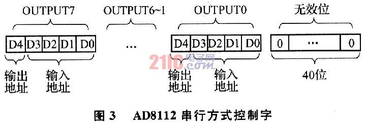
The AD8112 provides two programming modes, serial programming and parallel programming, which are selected by the high and low levels of the pin. When the serial programming mode is selected: the data of the DATA IN input is loaded on the falling edge of CLK, the data is latched on the falling edge of the data, and the matrix is ​​programmed; the DATA OUT is shifted by the 80-bit matrix mode register. When parallel programming is selected: the data input in parallel from D4 to D0 and the parallel input of A2 to A0 are loaded on the falling edge of CLK; the data is latched on the falling edge to program the matrix.
The AD8112 serial programming mode control timing diagram is shown in Figure 2. 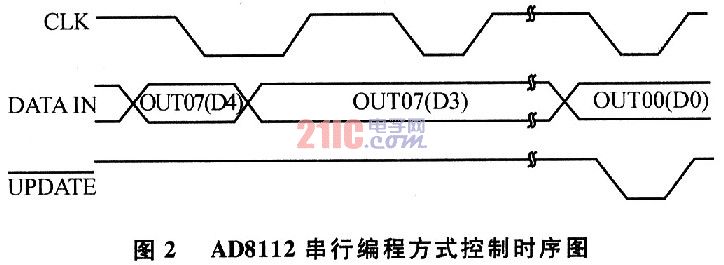
For a large matrix of N blocks of AD8112, these chips can be programmed with a series of N x 80 bit serial data streams. The AD8112 parallel programming mode control timing diagram is shown in Figure 4. 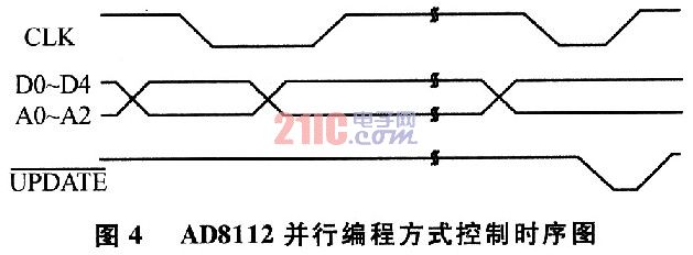
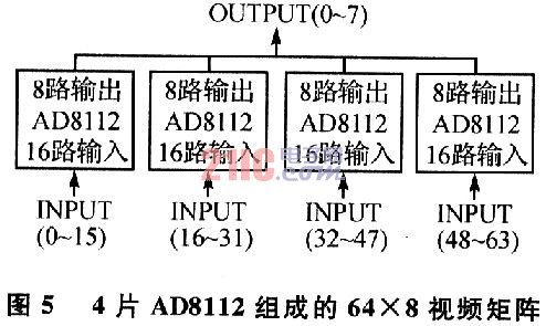
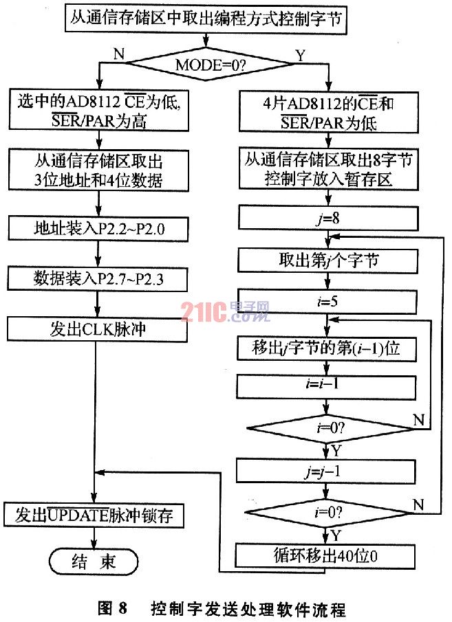
The connection between AD112 and LPC2378 in this video matrix is ​​shown in Figure 6. The DATA IN pin of the first AD8112 is connected to the P2.15 port on the LPC2378 to obtain the control command. The control word is sent to the four AD8112s by serial shift. The DATA OUT of each AD8112 is connected to the DATA IN of the adjacent chip. The P2.12~P2.14 pins of the LPC2378 are connected to the CLK of each AD8112, respectively, to provide control clock signals, serial parallel programming mode selection signals, and data latch signals. Pins P2.2 to P2.0 and P2.7 to P2.3 are connected to A2 to A0 and D4 to DO of each AD8ll2, respectively, to provide address and data signals for parallel programming. The P2.8~P2.11 pins are connected to the terminals of four AD8112s. You can program four chips at the same time for serial programming, or select one of the chips for parallel mode programming to control the video matrix switching array. 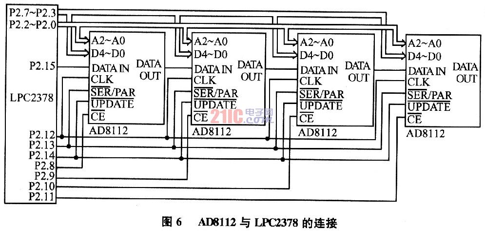
October 31, 2024