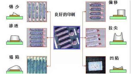
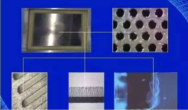
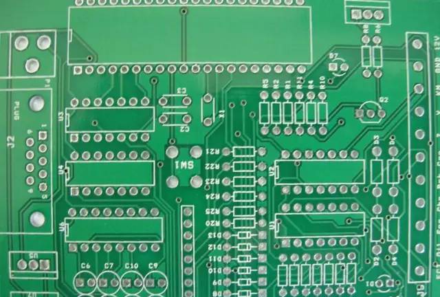
Drawing/tailing Drawing/tailing is a common defect in dispensing. The causes are usually too small, the dispensing pressure is too high, the distance between the plastic nozzle and the PCB is too large, the adhesive is out of date or the quality is not good, and the adhesive is applied. The viscosity is too good, it can't be restored to room temperature after taking out from the refrigerator, and the amount of dispensing is too large. Solution: Change the nozzle with larger inner diameter; reduce the dispensing pressure; adjust the "stop" height; change the glue, select the rubber of suitable viscosity; the patch glue should be restored to room temperature after being taken out of the refrigerator (about 4h) Put into production; adjust the amount of glue. Plastic nozzle blocked The fault phenomenon is that the glue nozzle has less glue or no glue point. The cause is generally that the pinhole is not completely cleaned; the paste glue is mixed with impurities, and there is plugging phenomenon; the incompatible glue is mixed. Solution: Change the clean needle; change the quality of the patch glue; the patch rubber grade should not be mistaken. Empty play The phenomenon is that only the dispensing action, but no glue amount. The reason is that the patch glue is mixed into the bubble; the nozzle is blocked. Solution: The glue in the syringe should be deaerated (especially the glue installed by itself); replace the nozzle. Component shift The phenomenon is that the component is displaced after the patch adhesive is cured. In serious cases, the component pins are not on the pad. The reason is that the glue of the patch glue is not uniform, for example, the chip component has more than one glue in the two points; When the component is displaced or the initial adhesive force of the patch glue is low; the PCB is placed for too long after dispensing, and the glue is semi-cured. Solution: Check if the nozzle is clogged, remove the uneven rubber; adjust the working condition of the placement machine; change the glue; the PCB placement time after dispensing should not be too long (less than 4h) Wave soldering will fall off The phenomenon is that the bonding strength of the components after curing is not enough, lower than the specified value, sometimes the film will appear to fall off. The reason is because the curing process parameters are not in place, especially the temperature is not enough, the component size is too large, and the heat absorption is large; The curing light is aging; the amount of glue is not enough; the component/PCB is polluted. Solution: Adjust the curing curve, especially to improve the curing temperature. Usually, the peak curing temperature of the heat curing adhesive is about 150 °C. If the peak temperature is not reached, it will cause the film to fall off. For the light curing glue, it should be observed whether the curing light is aging. Whether the lamp is black or not; the amount of glue and the contamination of the component/PCB are all issues that should be considered. Component pin floating/shifting after curing The phenomenon of this failure is that the component leads float or shift after curing. After the wave soldering, the tin material will enter the pad. In severe cases, short circuit and open circuit will occur. The main reason is uneven patch adhesive and patch adhesive amount. Excessive or patch component offset. Solution: Adjust the dispensing process parameters; control the amount of dispensing; adjust the processing parameters of the patch. Solder paste printing quality analysis The quality problems caused by poor solder paste printing are as follows: Insufficient solder paste (partial lack or even overall lack) will lead to insufficient solder joints in the solder joints, open components, component misalignment, and component erection. Solder paste adhesion will lead to short circuit and component misalignment after soldering. The overall offset of the solder paste printing will lead to poor soldering of the whole board components, such as less tin, open circuit, offset, vertical parts, etc. Solder paste tip is easy to cause short circuit after soldering. Main factors leading to insufficient solder paste When the printing press is working, the solder paste is not added in time. Solder paste quality is abnormal, which is mixed with foreign bodies such as hard blocks. The solder paste that has not been used up before has expired and is used twice. Board quality issues, there are inconspicuous covers on the pads, such as solder resist (green oil) printed on the pads. The fixed clamping of the board in the press is loose. Solder paste missing printed stencil is not thick and uneven. Solder paste leaked on the stencil or circuit board with contaminants (such as PCB packaging, stencil wiping paper, foreign matter floating in the ambient air, etc.). The solder paste scraper is damaged and the stencil is damaged. The equipment parameters such as pressure, angle, speed and demoulding speed of the solder paste scraper are not suitable. After the solder paste was printed, it was accidentally knocked out due to human factors. The main factors leading to solder paste adhesion Board design defects, pad spacing is too small. Stencil problem, the pupil position is not correct. The stencil is not wiped clean. The stencil problem causes the solder paste to fall off badly. Solder paste performance is poor, viscosity, collapse is unqualified. The fixed clamping of the board in the press is loose. The equipment parameters such as pressure, angle, speed and demoulding speed of the solder paste scraper are not suitable. After the solder paste is printed, it is squeezed and stuck due to human factors. The main factors leading to the overall deviation of solder paste printing The positioning reference point on the board is not clear. The positioning reference point on the board is not aligned with the reference point of the stencil. The fixed clamping of the board in the printing press is loose. The positioning thimble is not in place. The optical positioning system of the printing press is faulty. Solder paste missing stencil opening does not match the design file of the board. The main factors leading to the printing of solder paste tipping There are problems with the performance parameters such as solder paste viscosity. There is a problem with the demolding parameter setting when the board is separated from the missing screen board. 1. The hole in the hole of the stencil is burred. Patch quality analysis Common quality problems of SMT patches include missing parts, side parts, turning parts, offsets, and damages. The main factors that cause the patch to leak The component feeder is not in place. The air passage of the component nozzle is blocked, the nozzle is damaged, and the nozzle height is incorrect. The vacuum path of the equipment is broken and a blockage occurs. The board is not in good condition and is deformed. There is no solder paste or solder paste on the pads of the board. Component quality problems, the thickness of the same variety is inconsistent. The placement machine calls the program for errors or omissions, or the selection of the component thickness parameters is incorrect during programming. Human factors accidentally knocked out. The main factors that cause the SMC resistor to be turned over and side parts Component feed (feeder) feeding abnormal. The nozzle of the placement head is not the correct height. The height of the head pick is not correct. The size of the loading hole of the component tape is too large, and the component is flipped due to vibration. When the bulk material is placed in the braid, the direction is reversed. The main factors leading to component placement bias When the placement machine is programmed, the XY coordinate of the component is incorrect. The reason for the patch nozzle is that the suction is unstable. The main factors that cause damage to components The positioning thimble is too high, so that the position of the board is too high, and the components are squeezed during placement. When the placement machine is programmed, the Z coordinate of the component is incorrect. The nozzle spring of the placement head is stuck. Influencing factors of solder paste The quality of reflow soldering is affected by many factors. The most important factor is the temperature curve of the reflow soldering furnace and the composition parameters of the solder paste. Nowadays, the high performance reflow soldering furnace that is commonly used has been able to accurately control and adjust the temperature more conveniently. Curve. In contrast, in the trend of high density and miniaturization, the printing of solder paste becomes the key to the quality of reflow soldering. The particle shape of the solder paste alloy powder is related to the soldering quality of the narrow-pitch device. The viscosity and composition of the solder paste must also be selected appropriately. In addition, the solder paste is generally stored in a refrigerated state, and the cover should be opened after being taken to room temperature. Avoid mixing the solder paste into the water vapor due to the temperature difference. If necessary, stir the solder paste with a mixer. Impact of welding equipment Sometimes, the excessive vibration of the conveyor belt of reflow equipment is also one of the factors affecting the quality of welding. Influence of reflow soldering process After eliminating the abnormal quality of the solder paste printing process and the patch process, the reflow process itself also causes the following quality anomalies: Cold welding is usually less than the reflow temperature or the reflow zone. The temperature rise of the tin bead preheating zone is too fast (generally, the slope of the temperature rise is less than 3 degrees per second). Lianxi circuit board or components are damp, too much moisture is likely to cause tin explosion to produce tin. The crack is generally the temperature drop in the cooling zone is too fast (generally, the temperature drop slope of lead soldering is less than 4 degrees per second). In the re-flow welding of the tombstone phenomenon, the chip components often appear to rise. The reason for the occurrence: the root cause of the phenomenon of tombstoning is that the wetting force on both sides of the component is unbalanced, so the torque at both ends of the component is not balanced, which leads to the phenomenon of tombstoning. The following conditions can cause the wetting force imbalance on both sides of the component during reflow: ▶ The pad design and layout are unreasonable. If the pad design and layout have the following defects, it will cause the wetting force imbalance on both sides of the component. One of the two pads of the component is connected to the ground wire or has a large pad area on one side, and the heat capacity at both ends of the pad is not uniform; The temperature difference across the surface of the PCB is too large to cause uneven heat absorption on both sides of the component pad; Large devices QFP, BGA, and small chip components around the heat sink will have temperature unevenness at both ends. Solution: Change the pad design and layout. ▶ There is a problem with solder paste and solder paste printing. The activity of solder paste is not high or the solderability of components is poor. When the solder paste is melted, the surface tension is not the same, which will cause the pad wettability to be unbalanced. Uneven, more than one side will increase the heat absorbed by the solder paste, the melting time lags, so that the wetting force is not balanced. Solution: Use a higher activity solder paste to improve the solder paste printing parameters, especially the window size of the template. ▶ If the patch is displaced in the Z-axis direction, the force will be uneven, which will cause the component to be immersed in the solder paste. The depth of the solder will be uneven due to the time difference. If the component patch is displaced, it will directly lead to the tilt. monument. Solution: adjust the process parameters of the placement machine. ▶ The furnace temperature curve is not correct. If the reflow furnace body is too short and the temperature zone is too small, the working curve of the PCB heating will be incorrect, so that the wetness difference on the board surface is too large, resulting in unbalanced wetting force. Solution: Adjust the appropriate temperature curve according to each different product. ▶ Oxygen concentration in nitrogen reflow. Nitrogen protection and reflow will increase the wetting force of the solder, but more and more examples show that the phenomenon of tombstones increases when the oxygen content is too low; It is most suitable to control the oxygen content at the negative 6th power of (100~500)×10. Tin beads Tin beads are one of the common defects in reflow soldering. They not only affect the appearance but also cause bridging. Tin beads can be divided into two types, one of which appears on one side of the chip component, often an independent large spherical shape; One type appears around the IC pin and is in the form of scattered beads. There are many reasons for the generation of tin beads. The analysis is as follows: ▶ The temperature curve is incorrect. The reflow curve can be divided into four sections, namely preheating, heat preservation, reflow and cooling. The purpose of preheating and heat preservation is to raise the surface temperature of the PCB to 150 in 60~90s. °C, and keep warm for about 90s, which not only can reduce the thermal shock of PCB and components, but also ensure that the solvent of the solder paste can be partially volatilized, avoiding the splash caused by too much solvent during reflow soldering, causing the solder paste to rush out of the pad. Forming tin beads. Solution: Pay attention to the heating rate and take moderate warming to make it have a good platform to make the solvent volatilize. ▶ Quality of solder paste The metal content of solder paste is usually (90 ± 0.5) c / o, too low metal content will lead to too much flux composition, so too much flux will be caused by the pre-heating period is not volatile and cause flying beads. The increase in water vapor and oxygen content in the solder paste can also cause flying beads. Since the solder paste is usually refrigerated, when it is taken out of the refrigerator, if the recovery time is not ensured, water vapor will enter; in addition, the lid of the solder paste bottle is used every time. After the cover is tight, if not covered in time, it will also lead to the entry of water vapor. After the solder paste printed on the template is finished, the remaining part should be treated separately. If it is put back into the original bottle, it will cause the solder paste in the bottle to deteriorate and also produce tin beads. Solution: Choose high-quality solder paste, pay attention to the storage and use requirements of solder paste. ▶ Printing and patching In the solder paste printing process, due to the offset between the template and the pad, if the offset is too large, the solder paste will be immersed outside the pad, and the solder bead will easily appear after heating. In addition, the printing work environment is not good. Will also lead to the formation of tin beads, the ideal printing environment temperature is 25 ± 3 ° C, relative humidity is 50c / o ~ 65c / o. Solution: Carefully adjust the clamping of the template to prevent loosening. Improve the printing work environment. The pressure of the Z-axis during the patching process is also an important cause of the tin beads, but it often does not attract people's attention. The Z-axis head of the partial placement machine is positioned according to the thickness of the component, such as improper adjustment of the Z-axis height, The phenomenon that the solder paste is squeezed out of the pad at the moment when the component is attached to the PCB, this part of the solder paste will form a solder ball during soldering. In this case, the size of the solder ball is slightly larger. Solution: Re-adjust the Z-axis height of the placement machine. The thickness of the template and the size of the opening. The thickness of the template and the size of the opening are too large, which will lead to an increase in the amount of solder paste, which will also cause the solder paste to flow out of the pad, especially the template made by chemical etching. Solution: Select the appropriate thickness of the template and the opening size design, the general template opening area is the pad size of 90c / o. The wicking phenomenon, also known as core pulling, is one of the common soldering defects. It is more common in gas phase reflow soldering. The wicking phenomenon causes the solder to leave the pad and rise along the pin to the pin and the chip body, which usually forms a serious The phenomenon of the solder joint is caused by the high thermal conductivity of the component leads, so that the temperature rises rapidly, so that the solder preferentially wets the pins, and the wetting force between the solder and the leads is much greater than the wetting force between the solder and the pads. In addition, the upturn of the pin will increase the occurrence of wicking. Solution: For gas phase reflow soldering, the SMA should be fully preheated before being placed in the gas phase furnace; The solderability of the PCB pads should be carefully checked, and PCBs with poor solderability cannot be used for production; Pay full attention to the coplanarity of components, and devices with poor coplanarity cannot be used for production. In infrared reflow soldering, the organic flux in the PCB substrate and solder is a good absorption medium for infrared rays, while the pins can partially reflect infrared rays. Therefore, the solder preferentially melts, and the wetting force of the solder and the pad is Will be greater than the wetting force between the solder and the pin, so the solder will not rise along the pin, so the probability of wicking is much smaller. Bridge Bridging is one of the common defects in SMT production. It causes short circuits between components. It must be repaired when it encounters bridging. There are many reasons for bridging: ▶ Quality problems with solder paste. The metal content in the solder paste is too high, especially when the printing time is too long, and the metal content is likely to increase, resulting in bridging of the IC pins; The solder paste has a low viscosity and flows to the outside of the pad after preheating; The solder paste tower is poorly dropped, and flows to the outside of the pad after preheating; Solution: adjust the solder paste ratio or use a good quality solder paste. ▶ Printing system The printing machine has poor repeatability, misalignment (poor alignment of the steel plate, poor alignment of the PCB), causing the solder paste to be printed outside the pad, especially the fine pitch QFP pad; The template window size and thickness are not designed correctly, and the PCB pad design is uneven in Sn-pb alloy plating, resulting in more solder paste. Solution: adjust the printing press to improve the PCB pad coating; ▶ The pressure of the placement is too large, and the full flow of the solder paste is the most common cause in production. In addition, the accuracy of the patch is insufficient to cause the component to shift and the IC pin to be deformed. ▶ The reflowing furnace is heating up too fast, and the solvent in the solder paste is too late to volatilize. Solution: adjust the Z-axis height of the placement machine and the heating rate of the reflow oven. Wave soldering quality defects and solutions ▶ Pulling tip refers to the presence of excess needle solder at the end of the solder joint, which is a unique defect in the wave soldering process. Causes: improper PCB transfer speed, low preheating temperature, low tin bath temperature, low PCB transfer angle, poor peak, flux failure, poor solderability of component leads. Solution: adjust the transfer speed to the right, adjust the preheating temperature and the temperature of the pot, adjust the PCB transfer angle, preferably the nozzle, adjust the peak shape, replace the new flux and solve the lead solderability problem. ▶ Causes of solder joints: poor solderability of component leads, low preheating temperature, solder problems, low flux activity, too large pad holes, oxidation of the lead plates, contamination of the board surface, too fast transfer speed, tin pot temperature low. Solution: Solve the solderability of the lead, adjust the preheating temperature, test the tin and impurity content of the solder, adjust the flux density, reduce the pad hole during design, remove the PCB oxide, clean the board surface, adjust the transfer speed, adjust the temperature of the solder pot . ▶ Causes of tin thin: poor solderability of component leads, too large pads (except for large pads), too large pad holes, too large soldering angle, too fast transfer speed, high solder pot temperature, flux coating Uneven, the solder contains less than enough tin. Solution: Solve the solderability of the lead, reduce the pad and pad hole during design, reduce the soldering angle, adjust the transfer speed, adjust the temperature of the solder pot, check the pre-coating flux device, and test the solder content. ▶ Causes of leakage soldering: poor solderability of leads, unstable solder peaks, flux failure or uneven coating, poor solderability of PCB, jitter of transfer chain, incompatible flux and flux, and unreasonable process. Solution: Solve the solderability of the lead, check the wave device, replace the flux, check the pre-coating flux device, solve the PCB solderability (cleaning or return), check the adjustment transmission device, use the flux uniformly, adjust the process. ▶ After soldering, the solder mask of the printed board is foamed After welding, SMA will appear light green vesicles around individual solder joints. In severe cases, there will be foams of the size of the fingernails, which will not only affect the appearance quality, but also affect the performance in serious cases. This defect is also a reflow soldering process. The problem that often occurs in the middle, but the wave soldering time is more. Cause: The root cause of solder mask blistering is the presence of gas or water vapor between the solder mask and the PCB substrate. These traces of gas or water vapor can be entrained in different processes, when high temperature is encountered. The gas expands to cause delamination of the solder mask and the PCB substrate. When soldering, the pad temperature is relatively high, so the bubble first appears around the pad. One of the following reasons can cause the PCB to carry moisture: PCB often needs to be cleaned and dried in the process of processing, and then do the next process. If it is etched, it should be dried and then adhered to the solder mask. If the drying temperature is not enough, the water vapor will be entrained into the next process. Air bubbles appear at high temperatures. The storage environment before PCB processing is not good, the humidity is too high, and it is not dried in time when welding. In the wave soldering process, the aqueous flux is often used. If the preheating temperature of the PCB is not enough, the water vapor in the flux will enter the inside of the PCB substrate along the hole wall of the through hole, and the water vapor first enters the pad. After the high temperature of welding, air bubbles will be generated. Solution: Strictly control the various production links, the purchased PCB should be inspected and stored in the warehouse. Usually, the PCB should not be foamed within 10s at 260 °C. The PCB should be stored in a ventilated and dry environment for a period of not more than 6 months; The PCB should be pre-baked in an oven at (120 ± 5) °C for 4 hours before soldering. The preheating temperature in wave soldering should be strictly controlled. It should reach 100-140 °C before wave soldering. If water-based flux is used, the preheating temperature should reach 110-145 °C to ensure that the water vapor can be evaporated. After the SMA is welded, there is a nail-sized bubble. The main reason is that the inside of the PCB substrate is entrained with water vapor, especially the processing of the multi-layer board. Because the multi-layer board is pre-formed by a multi-layer epoxy resin prepreg and then hot pressed, If the storage period of the epoxy resin prepreg is too short, the resin content is not enough, and the pre-drying to remove the moisture is not clean, it is easy to entrain the water vapor after hot pressing. The half-solid film itself is not enough, the layer is between the layers. The bonding force is not enough to leave bubbles. In addition, after the PCB is purchased, the storage period is too long, the storage environment is humid, and the patch is not pre-baked before production. The damp PCB patch is also prone to blistering. Solution: After the PCB is purchased, it should be accepted after storage; the PCB should be pre-baked for 4 hours at (120 ± 5) °C. Open or short solder after IC pin soldering cause: Poor coplanarity, especially FQFP devices, which cause pin deformation due to improper storage. If the placement machine does not check the function of coplanarity, it is sometimes difficult to find. The solderability of the pins is not good, the IC storage time is long, the pins are yellow, and the solderability is not good, which is the main cause of the solder joints. Solder paste has poor quality, low metal content and poor solderability. Solder paste commonly used for soldering FQFP devices should have a metal content of not less than 90%. If the preheating temperature is too high, it will easily cause oxidation of the IC pin, which will deteriorate the solderability. The size of the print template window is so small that the amount of solder paste is not enough. Solution: Pay attention to the storage of the device, do not take the components or open the package. In the production, the solderability of the components should be checked. Pay special attention to the IC storage period should not be too long (within one year from the date of manufacture), and should be protected from high temperature and high humidity during storage. Carefully check the size of the stencil window, which should not be too large or too small, and be careful with the PCB pad size.
With 15+ years manufacturing experience for portable power.
Supply various portable charger for iPhone, Airpods, laptop, radio-controlled aircraft ,laptop, car and medical device mobile device, ect.
From the original ordinary portable power source to Wireless Power Bank, Green Energy Solar Power Bank, Magnetic Mobile Power, Portable Power Stations and other products continue to innovate.
Avoiding your devices run out of charge, Portable Chargers to keep your mobile device going.
We help 200+ customers create a custom mobile power bank design for various industries.
Portable Power Supply, Wholesale Powerbank,Portable Phone Charger,wholesale gifts TOPNOTCH INTERNATIONAL GROUP LIMITED , https://www.micbluetooth.com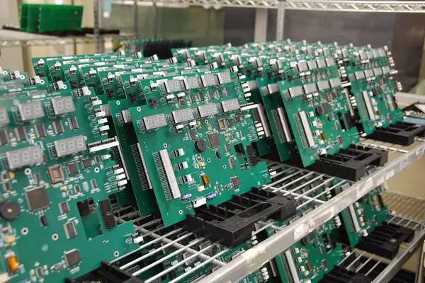


Common defects and solutions in the dispensing process
November 30, 2023