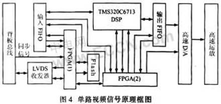
Hardware Design and Implementation of Radar Video Signal Simulator 2.3 Video signal card The video signal card is the core part of the entire system. Due to the large amount of calculation involved in the generation of the video signal, it is difficult for a single DSP to generate multiple video signals. At the same time, for the sake of system upgrade, each channel of the video signal simulator All use high-performance TMS320C6713 floating point digital signal processor. The DSP uses an advanced ultra-long instruction word structure, built-in 8 independent functional units, 2 fixed-point arithmetic logic units, 2 floating-point multipliers, 4 floating-point ALUs, 32 32-bit general purpose registers, 4 K words Section L1 high-speed program cache area, 4 K bytes of L1 high-speed data buffer, 256 K bytes of L2 two-level data buffer. This structure can maximize the parallel computing capabilities of 8 functional units, making the DSP performance under 300 MHz system clock work reach 2400MI / s and 1 800MFLO / s. The block diagram of single-channel video signal generation is shown in Figure 4. Among them, DSP completes the video signal operation; FPGA (1) is used to control the LVDS transceiver to receive commands, addresses and data from the bus, and before generating the video signal, download the clutter data, noise and target parameters generated by the host computer in advance Into the flash memory. During the generation of the video signal, FPGA (1) judges the working state of the DSP and reads the data of the Flash memory into the input FIFO; FPGA (2) mainly completes the logical conversion of the DSP input and output FIFO, and receives the video signal from the DSP to calculate Relative to the delay time of the PRF signal, receive the synchronization signal through the FPGA (1), read the data of the output FIFO and start the D / A converter; the DSP will input the data of the FIFO to its internal RAM, and generate it according to the corresponding data and target parameters The required video signal data, and write the calculated data to the output FIFO. FIFO uses IDT72V17160, and its read and write speed can reach 100 MHz. 3 system workflow The host computer generates off-line, azimuth difference, and pitch difference three-channel I / O clutter, noise, and target parameters according to the noise and clutter model. The host computer issues instructions and card addresses to download the data of each channel to the corresponding Flash Memory. Then, the host computer generates a DSP command, sends it to the cache of the main control card, triggers a synchronization signal, and sends the command to the DSP. At the same time, the video card generates a video signal according to the synchronization signal. The DSP samples and calculates the video signal, and then The results and status information are sent to the host computer for display. 3.1 Data download Data download is to download the clutter, noise data and target parameters generated in advance by the host computer to the corresponding Flash memory of each channel through the backplane bus. The entire transmission process is controlled by the host computer. The command, address, and data are formatted according to the format shown in Table 1. The order is sent to the main control card, and then the main control card FPGA controls the LVDS transceiver to send the command, address and data to the single-loop bus. After receiving the command from all bus nodes (video card), it will change to the data download working state , And then determine whether it is the node address. If yes, prepare to receive data, determine the area address, and write the data into the corresponding Flash partition; if not, close the data channel and wait to receive a new card address. Because the Flash memory needs a long programming time after writing 2 Kbytes of data, in the actual data download process, the polling method is used, that is, the host computer sends every 2 Kbytes of data before sending New card address, write data to the Flash memory of the next channel, and execute it in sequence until the first channel, the Flash memory programming is completed, and then continue to write data, saving data download time. 3.2 Generation of video signals The entire video signal generation process, data movement and signal operation are completed by the DSP. Since the TMS320C6713 DSP has 16 EDMA channels, it can quickly move data without occupying the CPU operating cycle, so the design is inside the DSP Open a ping-pong cache area (Ping PangCache), when the CPU calls the ping-pong cache data, EDMA moves the data to the ping-pong cache and exchanges it, so that EDMA data movement and CPU signal operation can be performed at the same time, ensuring real-time video signal generation. When the noise, noise and target parameters of each channel are downloaded, each channel FPGA (1) receives the instruction from the host computer and reads the data stored in the Flash into the input FIFO. The DSP starts the EDMA channel to read the input FIFO data to its internal ping pong In the cache. At this time, the DSP sends a READY signal to the FPGA (2), and the FPGA (2) connects the PRF synchronization signal to the external interrupt pin of the DSP, so that when the next PRF synchronization signal arrives, the DSP's external interrupt is triggered, and the DSP executes the internal waveform Operation program, and start the EDMA channel to move the clutter and other data to the ping-pong buffer. After the operation is completed, the DSP sends the target delay to the FPGA (2), and moves the completed waveform data to the output FIFO. After FPGA (2) receives the delay, when the next PRF synchronization signal arrives, it counts the DSP reception time, the count is over, reads the completed data from the output FIFO, and starts the D / A converter for data conversion. 3.3 Performance improvements Although the performance of the system can meet the actual application requirements, a slight improvement in some links will further enhance the functionality of the entire system. For DSP, the synchronous FIFO is asynchronous memory, so the DSP is set to asynchronous mode when reading and writing FIFO, the frequency of reading FIFO can only reach 25 MHz, and the frequency of writing FIFO can only reach 33 MHz. If the logic of the DSP read and write SDRAM timing is converted, the frequency of the read and write FIFO can reach 100 MHz, which greatly enhances the data throughput of the DSP; in addition, the data of the single-channel video signal uses only one flash memory, although the peak reading speed can reach 40 M bytes, but because every 2 K bytes read, Flash needs to occupy a cache time, so its average reading speed can only reach about 27 M bytes. If two Flashes are connected in parallel, the peak speed is reached, which improves the system performance. In addition, at present, only a ping-pong buffer is opened at the data input end of the DSP. If a ping-pong buffer is also opened at the data output end, the data can be moved. And the CPU operation is further executed in parallel to shorten the data processing time of each PRF cycle. 4 Conclusion Aiming at the specific radar signal processor, a hardware design of a video signal simulator is proposed. The simulator uses a combination of PC + DSP architecture. The entire system adopts a plug-in structure. The generation of each video signal uses a similar hardware circuit. The PC generates the required clutter, noise data and target parameters, and downloads the generated clutter, noise and target parameters of each video signal to the corresponding large-capacity flash through the self-designed adaptive single-loop bus in advance In the memory, after the data is downloaded, the real-time calculation is combined through the DSP, and the video analog signal is output under the trigger of each PRF synchronization signal. Since the Flash memory is a non-volatile memory, it has the advantage of not losing data after power-off, so if the clutter, noise, and target parameters do not change, the data only needs to be downloaded once. In addition, the use of the ring bus structure proposed in this article can ensure the rapid download of data. 2.3 Video signal card The video signal card is the core part of the entire system. Due to the large amount of calculation involved in the generation of the video signal, it is difficult for a single DSP to generate multiple video signals. At the same time, for the sake of system upgrade, each channel of the video signal simulator All use high-performance TMS320C6713 floating point digital signal processor. The DSP uses an advanced ultra-long instruction word structure, built-in 8 independent functional units, 2 fixed-point arithmetic logic units, 2 floating-point multipliers, 4 floating-point ALUs, 32 32-bit general purpose registers, 4 K words Section L1 high-speed program cache area, 4 K bytes of L1 high-speed data buffer, 256 K bytes of L2 two-level data buffer. This structure can maximize the parallel computing capabilities of 8 functional units, making the DSP performance under 300 MHz system clock work reach 2400MI / s and 1 800MFLO / s. The block diagram of single-channel video signal generation is shown in Figure 4. Among them, DSP completes the video signal operation; FPGA (1) is used to control the LVDS transceiver to receive commands, addresses and data from the bus, and before generating the video signal, download the clutter data, noise and target parameters generated by the host computer in advance Into the flash memory. During the generation of the video signal, FPGA (1) judges the working state of the DSP and reads the data of the Flash memory into the input FIFO; FPGA (2) mainly completes the logical conversion of the DSP input and output FIFO, and receives the video signal from the DSP to calculate Relative to the delay time of the PRF signal, receive the synchronization signal through the FPGA (1), read the data of the output FIFO and start the D / A converter; the DSP will input the data of the FIFO to its internal RAM, and generate it according to the corresponding data and target parameters The required video signal data, and write the calculated data to the output FIFO. FIFO uses IDT72V17160, and its read and write speed can reach 100 MHz. 3 system workflow The host computer generates off-line, azimuth difference, and pitch difference three-channel I / O clutter, noise, and target parameters according to the noise and clutter model. The host computer issues instructions and card addresses to download the data of each channel to the corresponding Flash Memory. Then, the host computer generates a DSP command, sends it to the cache of the main control card, triggers a synchronization signal, and sends the command to the DSP. At the same time, the video card generates a video signal according to the synchronization signal. The DSP samples and calculates the video signal, and then The results and status information are sent to the host computer for display. 3.1 Data download Data download is to download the clutter, noise data and target parameters generated in advance by the host computer to the corresponding Flash memory of each channel through the backplane bus. The entire transmission process is controlled by the host computer. The command, address, and data are formatted according to the format shown in Table 1. The order is sent to the main control card, and then the main control card FPGA controls the LVDS transceiver to send the command, address and data to the single-loop bus. After receiving the command from all bus nodes (video card), it will change to the data download working state , And then determine whether it is the node address. If yes, prepare to receive data, determine the area address, and write the data into the corresponding Flash partition; if not, close the data channel and wait to receive a new card address. Because the Flash memory needs a long programming time after writing 2 Kbytes of data, in the actual data download process, the polling method is used, that is, the host computer sends every 2 Kbytes of data before sending New card address, write data to the Flash memory of the next channel, and execute it in sequence until the first channel, the Flash memory programming is completed, and then continue to write data, saving data download time. 3.2 Generation of video signals The entire video signal generation process, data movement and signal operation are completed by the DSP. Since the TMS320C6713 DSP has 16 EDMA channels, it can quickly move data without occupying the CPU operating cycle, so the design is inside the DSP Open a ping-pong cache area (Ping PangCache), when the CPU calls the ping-pong cache data, EDMA moves the data to the ping-pong cache and exchanges it, so that EDMA data movement and CPU signal operation can be performed at the same time, ensuring real-time video signal generation. When the noise, noise and target parameters of each channel are downloaded, each channel FPGA (1) receives the instruction from the host computer and reads the data stored in the Flash into the input FIFO. The DSP starts the EDMA channel to read the input FIFO data to its internal ping pong In the cache. At this time, the DSP sends a READY signal to the FPGA (2), and the FPGA (2) connects the PRF synchronization signal to the external interrupt pin of the DSP, so that when the next PRF synchronization signal arrives, the DSP's external interrupt is triggered, and the DSP executes the internal waveform Operation program, and start the EDMA channel to move the clutter and other data to the ping-pong buffer. After the operation is completed, the DSP sends the target delay to the FPGA (2), and moves the completed waveform data to the output FIFO. After FPGA (2) receives the delay, when the next PRF synchronization signal arrives, it counts the DSP reception time, the count is over, reads the completed data from the output FIFO, and starts the D / A converter for data conversion. 3.3 Performance improvements Although the performance of the system can meet the actual application requirements, a slight improvement in some links will further enhance the functionality of the entire system. For DSP, the synchronous FIFO is asynchronous memory, so the DSP is set to asynchronous mode when reading and writing FIFO, the frequency of reading FIFO can only reach 25 MHz, and the frequency of writing FIFO can only reach 33 MHz. If the logic of the DSP read and write SDRAM timing is converted, the frequency of the read and write FIFO can reach 100 MHz, which greatly enhances the data throughput of the DSP; in addition, the data of the single-channel video signal uses only one flash memory, although the peak reading speed can reach 40 M bytes, but because every 2 K bytes read, Flash needs to occupy a cache time, so its average reading speed can only reach about 27 M bytes. If two Flashes are connected in parallel, the peak speed is reached, which improves the system performance. In addition, at present, only a ping-pong buffer is opened at the data input end of the DSP. If a ping-pong buffer is also opened at the data output end, the data can be moved And the CPU operation is further executed in parallel to shorten the data processing time of each PRF cycle. 4 Conclusion Aiming at the specific radar signal processor, a hardware design of a video signal simulator is proposed. The simulator uses a combination of PC + DSP architecture. The entire system adopts a plug-in structure. The generation of each video signal uses a similar hardware circuit. The PC generates the required clutter, noise data and target parameters, and downloads the generated clutter, noise and target parameters of each video signal to the corresponding large-capacity flash through the self-designed adaptive single-loop bus in advance In the memory, after the data is downloaded, the real-time calculation is combined through the DSP, and the video analog signal is output under the trigger of each PRF synchronization signal. Since the Flash memory is a non-volatile memory, it has the advantage of not losing data after power-off, so if the clutter, noise, and target parameters do not change, the data only needs to be downloaded once. In addition, the use of the ring bus structure proposed in this article can ensure the rapid download of data. Instrument Controller,Pressure Sensor,Temperature And Humidity Sensor,Control Pressure Sensor Xiaogan Yueneng Electronic Technology Co., Ltd. , https://www.xgsensor.com
November 28, 2023