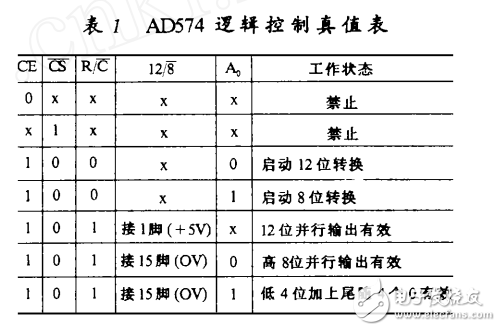
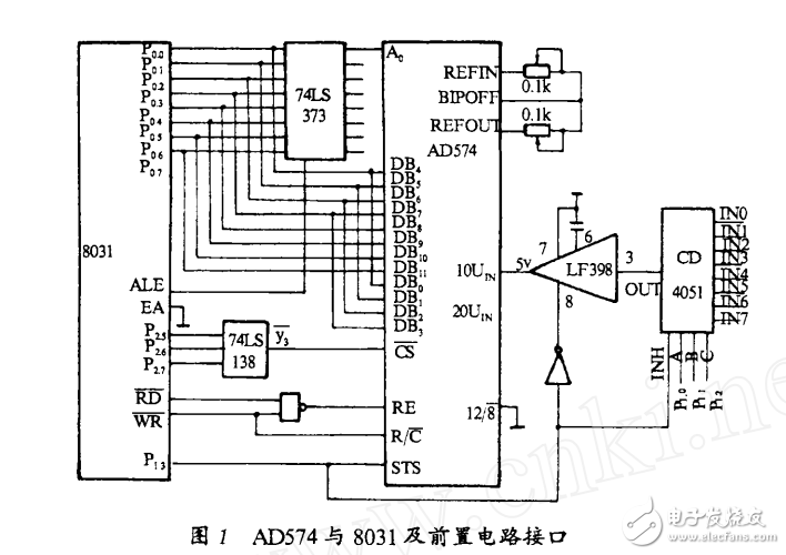
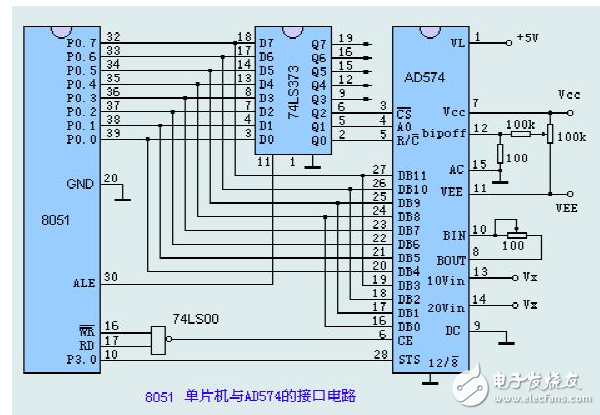
The AD574 is a 12-bit successive approximation fast A/D converter from Analog Devices, Inc. of the United States. Its conversion is 35us, and the conversion error is 0.05% of soil. It is a kind of A/D converter with wide application and moderate price in China. It has a three-state circuit that can be directly connected to various microprocessors and is compatible with CMOS and TTL levels without additional logic interface circuitry. The high-precision reference voltage source and clock circuit are internally configured, so that it can realize A/D conversion function without any external circuit and clock signal, and the application is very convenient. Many documents have an introduction to the interface technology between the AD574 and the 8031 ​​microcontroller, but the control function leads are basically limited to the connection of a single AD574 and 8031. Since the 8031 ​​has no internal program memory and its internal data memory is limited, the measurement and control system composed of the 8031 ​​often needs to expand the memory and the I/O interface chip. At this time, the single AD574 and 8031 ​​interface circuits are obviously Can not meet the requirements. In this paper, a practical data acquisition circuit interface between AD574 and 8031 ​​and pre-sampling control circuit is introduced. The main task of the A/D converter and the microcomputer interface is to perform A/D conversion according to the microcomputer instruction and send the converted data to the data bus of the microcomputer. Problems that need to be solved when the A/D converter is connected to the microcomputer 1. Data Output Buffering Problem The data bus of a microcomputer is a common channel for transferring data between a CPU and a memory and an I/O device. Therefore, when the A/D converter is connected to the microcomputer, the data output end of the A/D converter must be connected to the data bus through the tristate buffer. When not selected, the A/D converter output is in a high impedance state to avoid interference. Data transfer on the data bus. The AD574A chip has a three-state output buffer and the on-chip control timing can be combined with the microcomputer bus timing output so that it can be directly connected to the microcomputer data bus. 2. Generate chip strobe signal and control signal In the data acquisition system, in order to distinguish it from other I/O devices, the A/D converter must be given a specific address. The way in which the decoder that generates the address signal is connected to the address bus is determined by the I/O addressing mode used by the system and the address bus that it has. When the system adopts the memory mapping mode, the address code of the lower address line is usually transmitted by a 2-4 decoder, a 3-8 decoder, a 4-16 decoder, and a combination thereof, and can be selected according to specific conditions. Fixed or switch selectable address bus connections. 3. Reading data In order to extract the conversion result from the A/D converter, it is first necessary to consider the problem of the contact between the A/D converter and the microcomputer. The problem of the contact mode with the microcomputer is that the A/D conversion has to undergo a certain conversion time. The data read by the microcomputer is correct only after the end of the A/D conversion and the end of the conversion signal. In order to facilitate the microcomputer to check the switching state of the level change system, the contact and interrupt contact modes are usually adopted. Whether the query or interrupt mode is used in designing the A/D converter and the microcomputer interface circuit depends on the conversion time of the A/D converter used and the user's program arrangement. Generally speaking, when the A/D conversion time is short, the query mode should be adopted and the conversion time should be long. When the A/D574A is connected to the 8051 MCU, the A/D conversion can be performed by the query method. The AD574 has a reference voltage and clock circuit inside, which can perform A/D conversion independently without any external components, which provides great convenience. The analog signal input range is allowed to be selected between 0~+10V, 0~+20V and ±5V or ±10V, and the output is unipolar binary original code or bipolar offset binary code, which can complete 8-bit conversion. , can also complete the 12-bit conversion. Since the AD574 has a strong function, there are many control signals required to perform read and write operations. It has five control lines (CE, CS.R/C, 12/8, A). In order to facilitate reading this circuit, Its function is listed in Table 1. The AD574 is also provided with a flag status terminal STS. STS is high (BUSY) after the conversion is initiated and low (EOC) when the conversion is complete. The interface circuit between AD574 and 8031 ​​MCU, sample and hold device LF398 and multiplexer CD4051 is shown as in Fig. 1 (the external memory of 8031 ​​is not shown in the figure). In Figure 1, the POO of 8031 ​​is latched and connected to the A. terminal of AD574 to prevent A from changing during data reading. The output Y of the decoder 74LS138 serves as the chip select signal CS of the AD574, which can easily expand the peripheral chip of the circuit. CE is controlled by a NAND gate by the WR and RD signals, so CE is 1 regardless of the write state or the read state. The R/E signal is generated by WR. When the address operation of writing the AD574 port is performed, WR is low and the conversion is started. When the read command of the external RAM is executed, WR is high to complete the operation of reading the conversion result. 12/8 grounding, 12-bit conversion, the conversion result is read twice, and the left-aligned principle is followed when reading. The flag state end STS of the AD574 is typically used to perform when two transactions are used, one for reading the conversion result. When the query result data is read, the STS is connected to an -I/0 port line of the 8031 ​​(P.0 in Figure 1). The CPU directly queries the signal to judge the working state of the AD574. When the STS is high level. When turned low, the CPU can read the data. When the conversion result data is read by the interrupt method, the STS is connected to the external interrupt input terminal of the 8031. After the conversion is completed, the 8031 ​​is requested to interrupt and read the data. Of course, depending on the specific situation, the conversion result data is read by the delay (or timing) method without using the pin. The second is to use the signal as a sample of the sample/hold LF398 through the inversion to maintain the control signal. Here, according to the characteristics of the STS signal, the author also uses it as the disable input signal INH of the multiplexer CD4051. When AD conversion is performed, INH=1, the channel is disconnected, and the analog input is prohibited. When the A/D conversion ends, INH=0, the channel is turned on, allowing analog input, that is, making full use of the AD574 STS status terminal. The information can save a line of 8031, which is the preferred interface for the AD574 and the shunt switch. Regarding software programming, there are many introductions in the relevant literature, and the reader can easily write it according to the interface circuit, and will not be described here. The following figure shows the interface circuit between the 8051 MCU and the AD574A. The tristate latch 74LS373 and the 74LS00 NAND gate circuit are also used. The logic control signals are (, and A0). A data port P0 of the 8051 is issued and latched by the tristate latch 74LS373 to the outputs Q0, Q1 and Q2 for controlling the operation of the AD574A. The data output of the AD converter is also connected to the 8051 via the P0 data bus. Since we only use the 8-bit data port, the 12-bit data is read into the 8051 twice, so it is grounded. When p3.0 ​​of 8051 queries the STS end conversion signal, it reads the upper 8 bits of the converted 12-bit A/D data into 8051, and then reads the lower 4 bits into 8051. Regardless of whether the AD574A is in startup, conversion, and output, the enable CE must be 1. Therefore, the write control line and read control line of the 8051 are connected to the enable terminal CE of the AD574A through the NAND gate 74LS00. It is expected that with the continuous improvement of the design level and process level of the optocoupler, the performance is continuously improved, and the cost is gradually reduced, the application of the optocoupler in the analog circuit will be more and more. Privacy Hydrogel Screen Protector
The Privacy Screen Protector can display a black screen directly in front of the screen at an angle greater than 30° to effectively block the sight of people next to it, while achieving a perfect balance between black screen privacy and daytime clarity.
The Screen Protector can protect the edges and gaps of the display so that it can extend to the entire screen surface, thereby achieving maximum coverage without any exposed space.
The Self-Healing Screen Protector can provide the best protection for your phone from drops, bumps, scratches and normal wear and tear. Using an oleophobic waterproof coating can prevent sweat and grease from remaining on your fingerprints, keeping you simple all day long.
The 0.14mm thick Ultra-Thin Protective Film has a "real touch" feel and ensures fast response performance.
If you want to know more about Privacy Screen Protector products, please click the product details to view the parameters, models, pictures, prices and other information about Privacy Screen Protector.
Whether you are a group or an individual, we will try our best to provide you with accurate and comprehensive information about the Privacy Screen Protector!
Anti-peep Screen Protector, Privacy Screen Protector, Anti-spy Screen Protector, Privacy Protective Film, Privacy Hydrogel Film,Anti-peeping Screen Protector Shenzhen Jianjiantong Technology Co., Ltd. , https://www.jjthydrogelmachine.com


February 16, 2023