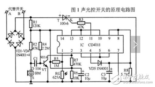
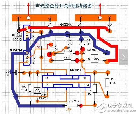
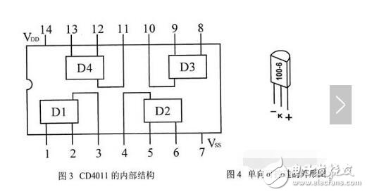
The integrated circuit CD4011 is a CMOS circuit containing four NAND gates. Each NAND gate has two inputs and one output. When one input has zero input, the output is 0. The output is only 1 when the input is 1. When both inputs are 0, the output is 1. This article mainly introduces the sound and light control delay switch circuit made by CD4011, which is introduced in detail from the working principle, component selection, installation and production, debugging, fault detection and maintenance. Let's take a look. The schematic diagram of the sound and light control delay switch is shown in Figure 1. The main component in the circuit is the digital integrated circuit cd4011, which contains four independent NAND gates vd 1~vd4, which makes the circuit structure simple and the operation reliability high. As the name suggests, the sound and light control delay switch uses the sound to control the "on" of the switch, and the delay switch "automatically closes" after a few minutes. Therefore, the function of the entire circuit is to turn on the sound signal and become the opening action of the electronic switch. After the signal flow direction of the circuit is clarified, the circuit can be divided into several units according to the main components, and the block diagram shown in FIG. 2 can be drawn. Figure 1 is analyzed in conjunction with Figure 2. The sound signal (footstep, applause, etc.) is received by the electret microphone bm and converted into an electrical signal, which is coupled to the base of vt by c1 for voltage amplification, and the amplified signal is sent to the NAND gate (vd1) pin 2, r4 R7 is the vt bias resistor and c2 is the power supply filter capacitor. In order to make the sound and light control switch open during the day, that is, the light is not bright, the light control circuit is composed of the photo resistor rg and other components, r5 and rg form a series voltage dividing circuit, and the resistance of the photoresistor is large when the environment is no light at night. The voltage at both ends of rg is high, that is, the high level is t=2πr8c3. Changing the value of r8 or c3 can change the delay time to meet different purposes. Vd3 and vd4 form a two-stage shaping circuit that shapes the square wave signal. When c3 is charged to a certain level, the signal is output to a high level after NAND gates vd3 and vd4, so that the unidirectional thyristor is turned on, and the electronic switch is closed; when c3 is fully charged, it is only discharged to r8, when discharging to a certain power Normally, the output of the NAND gates vd3 and vd4 is low, the one-way thyristor is turned off, the electronic switch is turned off, and a complete electronic switch is turned on and off. Diodes vd1~vd4 will bridge rectify AC 220v, become pulsating DC power, and step down by r1. After c2 filtering, it will be the DC power supply of the circuit, and supply power for bm, vt, ic, etc. Schematic: Board diagram: Use the sound and light control delay switch to replace the switch on the corridor of the residential area. Only after dark, when someone walks through the stairs and makes footsteps or other sounds, the corridor lights will automatically light up and provide illumination when people enter the house. Or walk out of the apartment, the corridor lights will automatically go out after a delay of a few minutes. During the day, even if there is sound, the corridor lights will not light up, which can save energy. The sound and light control delay switch is not only suitable for the corridors in residential areas, but also suitable for public places such as factories, office buildings, teaching buildings, etc. It has the advantages of small size, beautiful appearance, easy production, reliable work, etc., suitable for the majority of electronic enthusiasts. self made. Ic selects CMOS digital integrated circuit cd4011, which contains four independent NAND circuits. The internal structure is shown in Figure 3. vss is the negative pole of the power supply and vdd is the positive pole of the power supply. The thyristor t is made of 1 a/400v imported one-way thyristor type 1 00-6. If the load current is large, the unidirectional thyristor of 3a, 6a, 10a and other specifications can be selected. The shape of the unidirectional thyristor is as follows. As shown in Figure 4, its measurement method is: use r&TImes; 1 file, connect the red test lead to the negative pole of the thyristor, and connect the black test lead to the positive pole (as shown in the printed board diagram). At this time, the meter has no reading, then black. The pen touches the control pole k. At this time, the needle has a reading. When the black pen immediately leaves the control pole k, the needle still has a reading (note that when the control pole is touched, the positive and negative test leads are always connected to indicate that the thyristor is intact. Electret The small microphone used in the general recorder is selected. The measurement method is: use r&TImes; 100 files to connect the red pen to the outer casing s and the black pen to d, then use the mouth to blow against the electret, if the hands have a swing It shows that the electret is intact, the greater the swing, the higher the sensitivity; the photoresistor is 625a type, the resistance is 20k when there is light, and the resistance is greater than 100mq when there is no light, indicating that the component is intact. Rectifier diodes 1n4001 ~ 1n4007. In short, the choice of components can be flexible Grip, the parameters can be selected within a certain range. Other components can be labeled as shown in Figure 1. After preparing the complete set of components, use a multimeter to roughly measure the quality of each component (because it has been measured before leaving the factory). When welding, pay attention to soldering non-polar RC components first, the resistors are placed in a horizontal position, the capacitors are mounted in an upright position, close to the circuit board, and soldered with polar components such as electrolytic capacitors, microphones, rectifier diodes, triodes, unidirectional thyristors, etc. Do not install the components, pay attention to the correct polarity, otherwise the circuit can not work properly and even burn components. The printed circuit diagram is shown in Figure 5. Before debugging, carefully check the soldered circuit board against the printed circuit diagram, and do not have the phenomenon of wrong soldering, leakage soldering, short circuit, and component collision. After power-on, the human body is not allowed to touch any part of the circuit board to prevent electric shock and safety. If using a multimeter to detect, only use the two pens of the multimeter to touch the corresponding part of the circuit board. When debugging this circuit, please block the light of the photoresistor, connect ab to the switch position of the light, and tap the electret by hand. At this time, the light should be on. If the light is used to illuminate the photoresistor, then re-photograph the resident. Polar body, when the light is not bright, indicating that the photoresistor is in good condition, then the kit is successfully produced. If it is unsuccessful, please check carefully if there is any false soldering and dragging. The following faults may occur during commissioning. Maintenance should be carried out according to the specific circumstances. (1) The nighttime sound hours, the incandescent lamp EL does not light, and the light is on when the sound is loud. This is due to the reduced sensitivity of the sound signal input circuit. The reason may be that the sensitivity of the microphone MIC is lowered, the capacity of the capacitor C1 is decreased, the component parameters of the transistor T1, the resistors R2 and R3 are changed, and the like. During the inspection, the resistance of the resistor R1 can be appropriately reduced to increase the sensitivity of the MIC. Increase the resistance R2 and reduce the resistance of the resistor R3 to reduce the static operating point of the transistor T1. It is also possible to use an equivalent capacitor in parallel with C1 to observe whether the effect is changed or not, and to improve the sensitivity of the sound input circuit. (2) At night, the incandescent lamp EL often triggers and illuminates. This is generally caused by the sensitivity of the sound signal input circuit being too high. The components of the part of the circuit are adjusted in reverse to the above (1) during the inspection. (3) The incandescent lamp EL will illuminate when there is sound during the day. This is a malfunction of the optical signal input circuit. During the inspection, check whether the photoresistor Rg receives insufficient light. It can be used to remove the dust at the photoresistor Rg, check whether the position of the photoresistor Rg is correct, whether the photoresistor Rg is open, increase the resistance of the resistor R4, and reduce the NAND gate 1. The 1-terminal input level and other methods are solved. (4) The incandescent lamp EL does not illuminate when there is sound at night. The reason is that the sound signal input circuit cannot output a high level when there is sound, the light signal input circuit outputs a low level, and the integrated circuit IC1 is damaged. During the inspection, it is measured whether the two ends of the NAND gate 1 are at a high level when there is a sound signal, and whether the one end of the NAND gate 1 is at a high level when there is no light. If it is not high level, the fault is in the corresponding input circuit. If it is high level, check whether the logic relationship of IC1 is correct. (5) The incandescent lamps EL are bright during the day and night. The reason is generally that the two-way thyristor T2 is broken down. During maintenance, the electrical resistance between the two anodes of T2 is measured by the electric resistance of the multimeter after the power is cut off. If it is below 1KΩ, the two-way thyristor T2 has been broken down and should be replaced. (6) The delay time for the incandescent lamp EL to illuminate is not appropriate. If the delay time of the light is shortened, it may be caused by leakage of capacitor C3 or reduced capacity. Try using the same capacitor. If the delay time is not enough, the resistance of the resistor R8 may be appropriately increased, or the capacity of the capacitor C3 may be increased. Conversely, the resistance of the resistor R8 or the capacity of the capacitor C3 can be reduced. Fiber Optic Distribution Boxes Fiber Optic Distribution Boxes,Optical Distribution Box,Fiber Distribution Terminal,Optical Fiber Distribution Box CIXI LANGUANG PHOTOELECTRIC TECHNOLOGY CO..LTD , https://www.cxblueray.com


February 02, 2023