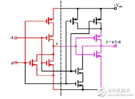
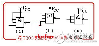
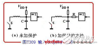
In order to avoid damage to the circuit due to electrostatic induction, the soldering iron used in soldering CMOS integrated circuits must be well grounded and the soldering time must not exceed 5 seconds. It is best to use 20~25W internal heating soldering iron and 502 epoxy flux, and use socket if necessary. The CMOS integrated circuit should not be mounted or removed with the power turned on. Where the process is in contact with the CMOS integrated circuit, the workbench and the floor used are not allowed to be paved with high-insulation boards (such as rubber sheets, glass sheets, plexiglass, rubber sheets, etc.), and a finely grounded steel wire mesh should be placed on the workbench. Or copper wire mesh and often check grounding reliability. All instruments and instruments of CMOS integrated circuits should be well grounded during testing. If it is a low-resistance signal source, ensure that the input signal does not exceed the power supply voltage range of the CMOS integrated circuit (7~15V for the CXXX series and 3~18V for the C4000 series), and VSS≤Vi≤VDD. If the input signal must exceed the supply voltage range of the CMOS integrated circuit, a current limiting resistor should be added to the input so that the input current does not exceed 5 mA to avoid the protection diode inside the CMOS integrated circuit from burning. If the signal source and the CMOS integrated circuit use two sets of power supplies, when starting up, the CMOS integrated circuit power supply should be connected first, and then the signal source power supply should be turned on. When shutting down, the signal source power should be turned off first, and then the CMOS integrated circuit power supply should be turned off. Because the input impedance of the CMOS integrated circuit is extremely high, the random static accumulation is likely to cause the voltage at any end of the circuit terminal to exceed the breakdown voltage of the MOS gate, thereby causing circuit damage. Therefore, when the CMOS integrated circuit is not in use, the outer leads of the circuit should be short-circuited or placed in a conductive shielding container to prevent electrostatic breakdown. Interchange of CMOS integrated circuits. Some CMOS integrated circuits can be directly used in use. For example, the domestic CC4000 can be directly replaced with the foreign products CD4000 and MC14000 series. For those CMOS integrated circuits in which the pin arrangement and package form are identical, but the electrical parameters are different, pay attention to it when switching. Such as some of the domestic CC4000 and CXXX, their working voltage is different, CC4000 is 3~18V, CXXX is 7~15V. Power supply and load capacity issues should be considered when switching. In addition, CMOS integrated circuits with different package types and pin arrangements are generally not directly replaceable. If you need to use it, you should make some corresponding transformations so that the two terminals with the same function have one-to-one correspondence. Solder CMOS integrated blocks. Look for a piece of aluminum foil and a flat foam that is slightly larger than the manifold. The aluminum foil is placed flat on the plastic foam, and the CMOS integrated block is vertically inserted into the foam and then pulled up, so that the aluminum foil is attached to the integrated block to short-circuit the pins. Then insert the integrated block into the specified position of the circuit board, solder it like other integrated blocks, and then tear off the aluminum foil after soldering. CMOS integrated circuits are highly susceptible to electrostatic charge due to their high input resistance. In order to prevent electrostatic breakdown, when the CMOS is produced, a standard protection circuit is added to the input terminal, but this does not guarantee absolute safety. Therefore, when using a CMOS integrated circuit, the following precautions must be taken. 1 Shielded when storing CMOS integrated circuits, usually placed in a metal container, or shorted by a metal foil. 2 CMOS integrated circuits can provide normal logic functions over a wide range of supply voltages, but the upper limit voltage of the power supply (even transient voltage) must not exceed the allowable limits of the circuit, ... the lower limit voltage of the power supply (even transient voltage) It is lower than the minimum value of the power supply voltage Vmin necessary for the system to work, and it must not be lower than VSS. 3 When soldering CMOS integrated circuits, generally use 20W internal heating type soldering iron, and the soldering iron should have a good grounding wire. It is also possible to quickly weld using the residual heat after the electric iron is turned off. Do not solder when the circuit is energized. 4 In order to prevent the input protection diode from being damaged due to forward bias, the input voltage must be between VDD and VSS, that is, VSS<u1<VDD. 5 When debugging the CMOS circuit, if the signal power supply and the circuit board use two sets of power supplies, the power of the circuit board should be turned on first, and then the signal source power supply should be turned on. When shutting down, the signal source power should be turned off first, and then the circuit board power supply should be turned off. That is, when the CMOS itself has not been powered on, input signal input is not allowed. 6 The extra input must never be left floating. Otherwise, it is not only vulnerable to external noise, but also the input potential is uncertain, which destroys the normal logic relationship and consumes a lot of power. Therefore, it should be handled separately according to the logic function of the circuit. For example, the redundant input of the AND gate and the NAND gate should be connected to VDD or high level; or the redundant input of the gate and NOR gate should be connected to VSS or low level; if the operating speed of the circuit is not high, no need When considering power consumption in particular, it is also possible to connect redundant inputs and terminals in parallel. As shown in Figure T308. The redundant inputs mentioned above include all inputs of the CMOS circuit that are not used but are powered. For example, there are four AND gates on a single integrated circuit. Only one of the circuits is used. All the inputs of the other three gates must be processed as redundant inputs. When the 7 input terminal is connected to the long line, due to the influence of distributed capacitance and distributed inductance, LC oscillation is easily formed, which may damage the input protection diode. Therefore, a 10~20kΩ protection resistor R must be connected in series at the input end, as shown in Figure T309. When the 8CMOS circuit is mounted on the printed circuit board, there is always an input terminal on the printed circuit board. When the circuit is pulled out from the machine, the input terminal must be suspended, so the current limiting protection resistor should be connected to each input terminal. T309 is shown. If a CMOS integrated circuit is to be mounted on a printed circuit board, the CMOS circuit must be installed after the other components associated with it are installed to prevent the CMOS device input from floating. 9 When plugging and unplugging the power plug of the circuit board, you should pay attention to cut off the power supply first to prevent the CMOS input protection diode from being burned out during the plugging and unplugging process. 1. Low static power consumption: The static power consumption of medium-scale circuits with a power supply voltage of VDD=5V is less than 100μW, which helps to improve integration and package density, reduce cost, and reduce power consumption. 2. Wide supply voltage range: The power supply voltage range of the 4000 series CMOS circuit is 3 to 18V, which makes the choice of power supply large and the power supply design requirements are low. 3. High input impedance: For a normally operating CMOS integrated circuit, the input protection diode is in a reverse bias state, and the DC input impedance can be greater than 100 MΩ. When the operating frequency is high, the influence of the input capacitance should be considered. 4. Strong fan-out capability: At low frequencies, one output can drive more than 50 CMOS device inputs, mainly due to the high input resistance of CMOS devices. 5. Strong anti-interference ability: The voltage noise tolerance of CMOS integrated circuits can reach 45% of the power supply voltage, and the noise tolerances of high level and low level are basically equal. 6. The logic swing is large: when no load occurs, the output high level VOH> VDD-0.05V, the output low level VOL < VSS + 0.05V. 7. CMOS integrated circuits also have better temperature stability and strong radiation resistance. The downside is that general CMOS devices operate at a lower speed than TTL ICs, and power consumption increases significantly with increasing operating frequency. 1. Power connection and selection: VDD terminal is connected to the positive pole of the power supply, and VSS terminal is connected to the negative pole of the power supply (ground). Never make a mistake, otherwise the device will be damaged due to excessive current. For the series of power supply voltage range of 3V ~ 18V series. For example, in the CC4000 series, VDD is usually connected to +5V power supply in the experiment, and VDD voltage is selected in the middle value of the power supply variation range. For example, if the power supply voltage varies between 8 and 12V, it is appropriate to select VDD=10V. Note: When CMOS devices operate at different VDD values, their output impedance, operating speed, and power consumption are all subject to change and must be considered in the design. 2. Input processing: The extra input cannot be left floating. VDD or VSS should be connected as required by logic to avoid logic confusion and even damage the device. When the working speed is not high, and the load capacity is required, the input terminals can be used in parallel. For CMOS devices mounted on a printed circuit board, in order to avoid the input terminal from floating, the current limiting resistor RP and the protection resistor R should be connected to the input end of the circuit board. When VDD=+5V, the RP takes 5.1KΩ, and R generally takes 100KΩ ~ 1MΩ. 3. Output processing: The output terminal is not allowed to directly connect to VDD or VSS. Otherwise, the device will be damaged. Except for the three-state (TS) device, two different chip outputs are not allowed to be used in parallel, but sometimes in order to increase the driving capability, on the same chip. The outputs can be connected in parallel. 4. The requirements of the input signal VI: VI high level VIH < VDD, VIL low level VIL is lower than the circuit allows low voltage; when the device VDD end is turned on, signal input is not allowed, otherwise the input will be protected The diode in the circuit is damaged. 5. A protection diode is connected between the input end of the CMOS device and VSS. In addition to some interface circuits such as a level converter, a protection diode is also connected between the input terminal and the positive power supply VDD. Therefore, during normal operation and soldering of the CMOS device, The device is generally not damaged by the induced charge. However, when using a CMOS digital integrated circuit, the low level of the input signal cannot be lower than (VSS-0.5V). Except for some interface circuits, the high level of the input signal must not be higher than (VDD+0.5V), otherwise It may cause the protection diode to turn on or even damage and may damage the input stage.
Instruction Manual
1. Features
Clock display, 10 sets of adjustable timed power control, randomized power control, manual switch and optional DST setup.
2. First time charging
This timer contains a rechargeable battery. It is normal that the new/old model runs out of battery if it wasn`t being charged for a long period of time. In this case, the screen will not turn on.
To charge : simply plug the timer to a power outlet. The charging time should take at least 15 minutes.
If the screen doesn`t light up or displays garbled characters, simply reboot the system by pressing the [RESET" button.
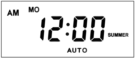
3. Set clock
Hold [CLOCK" button and [WEEK" button to adjust week.
Hold [CLOCK" button and [HOUR" button to adjust hour.
Hold [CLOCK" button and [MINUTE" button to adjust minute.
Hold [CLOCK" button and [TIMER" button to select 12 hour/24 hour display.
Hold [CLOCK" button and [ON/AUTO/OFF" button to enable/disable DST (daylight-saving-time).
4. Set timer
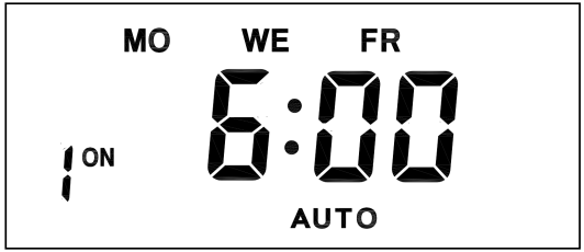
Press [TIMER" button, select and set timer. Setting rotation : 1on, 1off, 2on, 2off, ...... , 10on, 10off.
Press [HOUR" button to set hour for timer.
Press [MIN" button to set minute for timer.
Press [WEEK" button to set weekday for timer. Multiple weekdays can be selected. ex: if selected [MO", the timer will only apply on every Monday; if selected [ MO, WE, FR", the timer will apply on every Monday, Wednesday and Friday.
Press [RES/RCL" button to cancel the selected on or off timer. The screen will show "-- -- : -- --" , the timer is canceled.
Press [RES/RCL" button again to reactivate the timer.
When timers are set, press [CLOCK" to quit timer setting and return to clock.
5. Random function
Press [RANDOM" button to activate random function, press again to cancel function.
System only runs random function when [AUTO" is on.
Random function will automatically start the timer from 2 to 32 minutes after the setting.
ex : if timer 1on was set to 19:30 with the random function on, the timer will activate randomly between 19:33 to 20:03.
if timer 1off was set to 23:00 with the random function on, the timer will activate randomly between 23:02 to 23:32.
To avoid overlapping, make sure to leave a minimum of 31 minutes gap between different sets of timer.
6. Manual control
Displayed features:
ON : socket turns on.
OFF : socket turns off.
AUTO : socket turns on/off automatically via timer.
Manual ON setting
Press [ON/AUTO/OFF" button to switch from [AUTO" to [ON".
This mode allows socket of the device to power up. Power indicator will light up.
Manual OFF setting
Press [ON/AUTO/OFF" button to switch from [AUTO" to [OFF".
This mode turns socket of the device off. Power indicators will turn off.
7. Electrical parameters
Operating voltage : 230VAC
Battery : NiMh 1.2V
Power consumption : < 0.9W
Response time : 1 minute
Power output : 230VAC/16A/3680W
Q&A
Q: Why won`t my timer turn on?
A: It`s out of battery, you can charge the timer by plugging onto any power outlet. Charge the device for at least 15 minutes. Then press [RESET " button to reset the device.
Q: Can I set seconds of the timer?
A: No, the smallest time unit is minute.
Q: Does my timer keeps old settings without being plugged onto a power outlet?
A: Yes, the timer has an internal battery, it allows the timer to save settings without a power outlet.
Q: Is the battery rechargeable?
A: Yes, the battery is rechargeable. We recommend to charge it for 4 hours so the battery is fully charged.
Q: Does the timer needs internet connection?
A: The timer does not need internet.
Q: Does the screen have back light function?
A: It doesn`t support back light.
Digital Timer Socket, Timing Switch Socket, Electronic Timer Socket, Timer Socket NINGBO COWELL ELECTRONICS & TECHNOLOGY CO., LTD , https://www.cowellsockets.com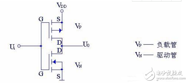


March 10, 2023